| Equipment |
Purpose |
Key Specifications |
| Automatic Wire Bonder |
Precision electrical interconnection |
Nanometre-level positioning, supports confined�cavity operation, wedge-bond mode |
| Eutectic Die Bonder |
High-precision chip placement |
Placement tolerance ±1-3 µm |
| Plasma Cleaner |
Surface activation of bond pads |
Removes oxides and organic residues |
| Automatic Optical Inspection (AOI) System |
Bond quality inspection |
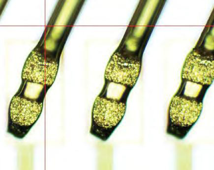
Inspects stitch shape and wire loop profile |
| Ball Shear / Wire Pull Tester |
Bond strength verification |
Evaluates bonding reliability |
Typical Applications
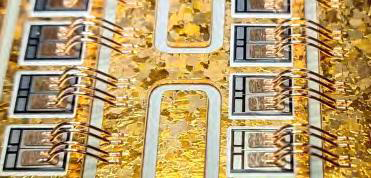
- Optical transceivers – High-density, multi-channel wire bonding in COB (chip-on-board) integration for high-speed modules
- Laser diodes – High-power, long-haul optical communication devices in butterfly packages, requiring multiple signal, temperature-control, and power supply wire bonds
- Photodiodes – TO-can packages with wedge bonding interconnections
- VCSEL modules – LiDAR and 3D-sensing applications requiring lens alignment and multi-channel parallel wire bonding; gold wire bonding is the preferred interconnection for VCSEL top contacts
- LiDAR components – Electrical wire bonding for complex devices such as 128-channel optical phased arrays (OPA)
-
Infrared sensors and detectors – Demanding high consistency in bond strength
How to Choose a Wire Bonder for Optical Devices
| Device |
Recommended Machine |
Item |
| VCSEL |
Automatic Wedge Wire Bonder |
HY-WB900 |
| Laser Diode |
Precision Wedge Bonder |
HY-WBH790 |
| Photodiode |
Ball/Wedge Wire Bonder |
HY-LS3000 |
| Optical Transceiver |
High-Speed Automatic Wire Bonder |
HY-WB700P |
| LiDAR Module |
Multi-Channel Wire Bonder |
HY-HW3850 |
Why Choose Hyrnus
- 17+ Years Experience
- Customized Solutions
- Global Technical Support
- 50+ R&D and Technical Engineers
- 40+ Countries and Regions Served
- 200+ Projects Delivered
Looking for a Complete Optical Device Packaging Solution?
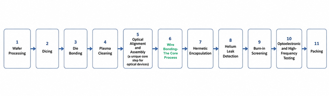
Optical device wire-bonding packaging involves multiple core processes – precision die attachment, optical alignment, wedge bonding, and hermetic sealing – each demanding specialised equipment and process expertise. The Hyrnus team is dedicated to providing comprehensive solutions for the optoelectronics industry, covering equipment selection, process optimisation, and production support.
Contact our engineering team
FAQs
Why is wire bonding used in optical devices packaging?
Wire bonding provides reliable, low-resistance electrical interconnections, with the added advantages of mature processes, highly automated equipment, and suitability for high-volume production. For temperature-sensitive devices such as VCSELs, wire bonding can be performed at low temperatures without degrading optoelectronic characteristics.
Can copper wire be used for optical device wire bonding?
Yes. Copper wire offers lower cost and better thermal conductivity, but it is prone to oxidation and has a narrower process window. In optical device packaging, gold wire remains the highest-reliability option. The choice of wire material should be evaluated based on package design, process requirements, and reliability targets.
How dose optical-device wire bonding differ from standard IC wire bonding?
Key differences include:
(1) Optical devices almost exclusively use wedge bonding rather than ball bonding to reduce parasitic inductance;
(2) Bonding stress must be more tightly controlled to avoid damage to optical facets;
(3) Low-temperature bonding is required to protect semiconductor materials;
(4) Loop height must be strictly controlled to prevent contact with the lid or housing.
How can wire-bonding reliability be ensured?
Reliability should be controlled through:
(1) Optimisation of process parameters – ultrasonic power, bonding force, and bonding time;
(2) Maintaining clean and well-metallised bond pad surfaces;
(3) Strict control of loop height and shape to avoid short circuits or contact with the package;
(4) Verification via ball-shear/wire-pull tests and burn-in screening. Studies show that bond-wire height, diameter, and curvature significantly affect bonding stress.