leave a message
If you are interested in our products and want to know more details,please leave a message here,we will reply you as soon as we can.



Soft solder die attach is a widely established joining process for power semiconductor packaging. It creates both a mechanical bond and a thermal-electrical path between a semiconductor die and a leadframe, copper substrate, ceramic substrate, or module baseplate. Because the die attach layer directly affects heat dissipation, electrical resistance, mechanical stress, and package reliability, stable control of solder volume, wetting, bond-line thickness, die tilt, atmosphere, and cooling is essential.
This application guide explains where soft solder die attach is used, how the process works, which defects require the most attention, and what equipment capabilities should be evaluated before selecting a production solution.
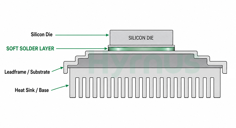
Soft solder die attach uses a low-melting-point metal alloy, usually based on tin and combined with elements such as silver, lead, indium, or bismuth, to form a metallurgical joint between the die backside and the package carrier. In soldering terminology, filler metals with melting temperatures below 450°C are generally classified as soft solders.
The process is completed under a controlled combination of temperature, time, placement force, and atmosphere. Once the solder melts and wets both surfaces, the assembly is cooled to solidify the joint. The resulting layer must transfer heat and current while accommodating thermo-mechanical stress caused by differences in the coefficients of thermal expansion of the die, solder, and carrier materials.
Soft solder die attach is commonly selected for power packages that require an efficient thermal path and a reliable backside connection. Typical applications include:
The suitability of soft solder depends on the package structure, operating temperature, power cycling requirement, compliance standard, substrate metallization, and target cost. For applications with exceptionally high junction temperatures or demanding power-cycle requirements, alternative die attach technologies may also need to be evaluated.
The exact sequence varies according to the solder form and package design, but a typical automated process includes the following stages.
Step 1: Leadframe or Substrate Preheating
The leadframe or substrate enters a heated track or bonding station. Preheating reduces thermal shock, supports solder melting, and prepares the attach area for stable wetting. In some continuous soft-solder systems, the heated process zone may operate in the 300-400°C range; the actual setpoint and interface temperature must be matched to the solder alloy, package mass, and required thermal profile.
Step 2: Solder Feeding and Forming
A controlled amount of solder is delivered to the attach position. When solder wire or ribbon is used, the equipment cuts or feeds a defined length according to the die size and required solder volume. A forming tool or stamp may then spread the molten solder into a repeatable shape before die placement.
Step 3: Die Pick-Up, Alignment, and Placement
A vacuum collet picks the singulated die from the wafer or carrier. The vision system identifies the die and target position, applies alignment correction, and places the die onto the molten or prepared solder layer with controlled force.
Step 4: Bond Formation and Cooling
Temperature, dwell time, and placement force are controlled to promote wetting and metallurgical bonding. The assembly then moves through a controlled cooling zone so the solder solidifies without excessive die movement, tilt, or residual stress.
Step 5: Inspection and Process Verification
Depending on the production line, inspection may include die-position verification, die-tilt measurement, bond-line evaluation, surface inspection, and X-ray analysis for voids. Process data can also be linked to product identification for traceability.
Common Solder Feeding Options
| Solder Form | Main Characteristic | Typical Use |
| Solder wire | Continuous reel feeding and programmable length control | High-volume production with repeatable die sizes |
| Solder ribbon | Flat geometry and controlled width | Specific package or die formats |
| Preformed solder | Defined shape and volume | Applications requiring tight solder-volume control |
| Solder paste | Printed or dispensed before placement | Special process flows or substrate configurations |
4.1 Void Control
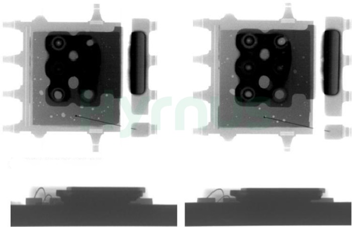
Voids are among the most important quality concerns in a solder die attach layer because they interrupt heat flow and can create localized hot spots. They may result from trapped gas, incomplete wetting, surface contamination, poor solder-volume distribution, or volatile residues when paste or flux-containing materials are used.
Practical void-reduction measures include:
4.2 Wetting and Oxidation Control
Good wetting is required to form a continuous metallurgical interface. Oxidized solder, die metallization, or leadframe surfaces can cause non-wetting, incomplete coverage, and unstable bond strength. Enclosed heated tracks, controlled nitrogen flow, low-oxygen monitoring, and validated surface preparation help reduce oxidation-related defects. Forming gas may be used in qualified processes, but gas composition and safety controls must follow the equipment and factory requirements.
4.3 Bond-Line Thickness and Die Tilt
Bond-line thickness influences thermal resistance, stress distribution, and mechanical reliability. Excessive variation can also lead to die tilt, which affects downstream wire bonding and package geometry. Repeatable solder volume, controlled forming, accurate placement force, collet condition, and stable cooling are all important for maintaining a uniform joint.
4.4 Temperature, Force, and Time
The process window should be developed for the specific alloy, die size, package mass, and surface finish. The following values are useful as an initial equipment-capability reference rather than universal production settings:
| Parameter | Illustrative Range | Main Influence |
| Heated process zone | Approximately 300-400°C in some systems | Solder melting, wetting, oxidation, and void behavior |
| Placement or bond force | Approximately 30-500 g in the source process range | Solder spreading, bond-line thickness, die tilt, and die stress |
| Bond or dwell time | Several seconds, process dependent | Wetting and metallurgical joint formation |
| Oxygen level | Low-oxygen control; some systems target below 200 ppm | Oxidation prevention and process repeatability |
| Observed Issue | Possible Causes | Process Response |
| High voiding | Trapped gas, contamination, poor wetting, excessive volatile content, unsuitable thermal profile | Improve surface preparation, atmosphere control, thermal profiling, solder-volume control, and X-ray verification |
| Die tilt | Uneven solder distribution, inconsistent force, worn collet or forming tool, movement during cooling | Stabilize solder forming, placement force, tooling condition, and cooling |
| Insufficient solder coverage | Low solder volume, feeding error, non-wetting, inaccurate target position | Calibrate feeding length, inspect surfaces, verify vision alignment, and monitor solder shape |
| Solder overflow | Excess solder, high force, excessive temperature or dwell time | Reduce solder volume, optimize force, and tighten thermal controls |
| Die shift | Unstable placement, excessive solder flow, vibration, or uncontrolled cooling | Optimize placement motion, dwell, transport stability, and cooling |
| Oxidation or non-wetting | High oxygen level, contaminated surfaces, unsuitable metallization or profile | Improve atmosphere monitoring, cleaning, material compatibility, and profile development |
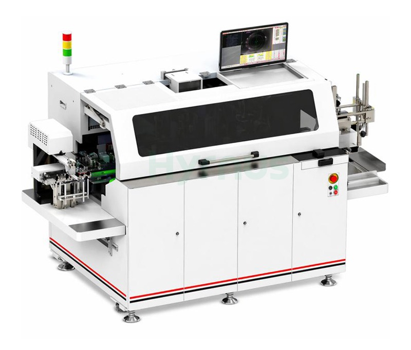
A complete production system must coordinate die handling, solder delivery, thermal processing, atmosphere control, and inspection. Key subsystems typically include:
Equipment Selection Checklist
| Selection Area | Questions to Confirm |
| Package and substrate compatibility | Confirm leadframe width, strip format, substrate type, package family, and heating method. |
| Die and wafer range | Check minimum and maximum die size, die thickness, wafer size, wafer-frame format, and die-eject capability. |
| Solder material and form | Verify alloy compatibility and whether the machine supports wire, ribbon, preform, or paste. |
| Placement performance | Evaluate accuracy, repeatability, force control, die rotation, and actual cycle time for the target product. |
| Thermal process capability | Review heating-zone design, temperature uniformity, recipe control, dwell time, and cooling stability. |
| Atmosphere control | Confirm chamber sealing, nitrogen or qualified forming-gas support, oxygen monitoring, exhaust, and safety design. |
| Quality control | Assess die-tilt measurement, solder-shape inspection, X-ray integration, alarms, SPC, and traceability options. |
| Changeover and maintenance | Review tooling replacement, recipe switching, consumable access, cleaning, and preventive-maintenance requirements. |
| Factory integration | Confirm upstream and downstream interfaces, MES or SECS/GEM requirements, data formats, and line-layout constraints. |
Soft solder die attach remains an important process for power semiconductor packaging because it combines effective thermal and electrical performance with a mature production foundation. Reliable results depend not only on the solder alloy, but also on surface condition, solder-volume control, atmosphere, thermal profiling, placement force, die alignment, and controlled cooling.
When evaluating a production system, the equipment should be matched to the package format, die and wafer range, solder form, throughput target, inspection plan, and factory integration requirements. Process capability should be verified with application trials rather than selected from headline specifications alone.
HYRNUS provides semiconductor packaging equipment and process-oriented configuration support for power device manufacturing. Explore our die bonding equipment solutions for compatible die attach platforms and supporting process modules.
For package-specific process evaluation, equipment configuration, or line-integration requirements, contact our engineering team with your die size, wafer format, package type, solder material, target capacity, and quality requirements.
FAQ
It creates a mechanical, thermal, and often electrical connection between the semiconductor die and the leadframe, substrate, or module baseplate.
Common options include solder wire, ribbon, preforms, and solder paste. The choice depends on the package design, solder-volume tolerance, throughput, and process flow.
Voids interrupt the heat-transfer path and can concentrate temperature in localized areas. Their size, location, and distribution should be evaluated by X-ray inspection.
It may be suitable for some package designs, but high-junction-temperature and demanding power-cycle applications often require comparison with sintered silver or other advanced attach materials.
leave a message
Scan To Wechat :

Scan To WhatsApp :