Enter product details (such as color, size, materials etc.) and other specific requirements to receive an accurate quote.
leave a message
If you are interested in our products and want to know more details,please leave a message here,we will reply you as soon as we can.

other
2025 Global Semiconductor Materials Market: Size, Growth and Key Trends

2025 Global Semiconductor Materials Market: Size, Growth and Key Trends

June 30, 2026
 Key Takeaways 
  • Global semiconductor materials revenue reached $73.2 billion in 2025, up 6.8% year over year.
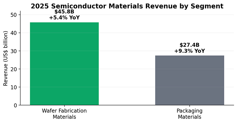
  • Packaging materials grew 9.3%, faster than wafer fabrication materials at 5.4%.
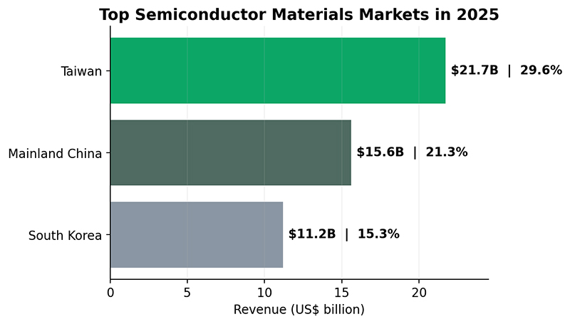
  • Taiwan, Mainland China and South Korea together represented approximately 66.3% of global materials revenue.
  • AI, high-performance computing, HBM and advanced packaging are increasing material intensity and process complexity.
  • The trend raises requirements for precision, reliability, automation and traceability in packaging and testing equipment.
 
The global semiconductor materials market reached a new record of $73.2 billion in 2025, representing year-over-year growth of 6.8%. According to SEMI’s Materials Market Data Subscription, both wafer fabrication materials and packaging materials expanded as manufacturers increased investment in advanced processes, high-performance computing and high-bandwidth memory production.
The headline number is important, but the market structure provides a more useful signal for equipment manufacturers and semiconductor production companies. Packaging materials grew materially faster than wafer fabrication materials, while the leading Asian manufacturing regions continued to account for most global consumption. These changes point to greater demand for advanced substrates, reliable interconnects, tighter process control and more capable packaging and testing systems.


1. 2025 Semiconductor Materials Market at a Glance


Market Segment 2025 Revenue YoY Growth Share of Total
Total Semiconductor Materials $73.2 billion 6.80% 100%
Wafer Fabrication Materials $45.8 billion 5.40% 62.60%
Packaging Materials $27.4 billion 9.30% 37.40%
*Source: SEMI. Segment shares calculated by HYRNUS based on reported 2025 revenue.


2. Wafer Fabrication Materials Continued to Expand
Wafer fabrication materials revenue increased 5.4% to $45.8 billion in 2025. SEMI reported strong double-digit growth in lithography-related materials, including photomasks, photoresists and ancillary materials, as well as wet chemicals.
The result reflects a broader increase in process intensity. Advanced manufacturing nodes require tighter lithography control, more demanding cleaning and surface preparation steps, and strict management of material purity and consistency. As the number and complexity of process steps increase, material consumption can rise even when wafer starts do not grow at the same rate.
For semiconductor manufacturers, this means that material selection and equipment capability must be evaluated together. Stable chemical delivery, contamination control, process repeatability and data traceability all become more important as process windows narrow.


3. Packaging Materials Outpaced Wafer Fab Materials
Packaging materials revenue grew 9.3% to $27.4 billion, accounting for approximately 37.4% of the total semiconductor materials market. Substrates and bonding wire were the leading contributors to growth. Advanced substrate demand supported the increase, while higher gold prices also lifted bonding wire revenue.
The growth of advanced packaging is increasing demand for high-density routing, fine-pitch interconnection, thermal management and reliable multi-die integration. Technologies such as 2.5D and 3D integration, chiplet-based architectures and HBM place greater emphasis on substrates, interposers, bonding interfaces, underfill materials and heat dissipation solutions.
As packaging structures become more complex, production equipment must maintain accuracy across more variables. Die placement, bonding energy, wire-loop consistency, surface condition, molding quality and test coverage can all affect final device yield and reliability.


4. Regional Semiconductor Materials Market Landscape
Taiwan remained the world’s largest semiconductor materials market for the 16th consecutive year, generating $21.7 billion in revenue in 2025. Mainland China ranked second at $15.6 billion, supported by double-digit growth, followed by South Korea at $11.2 billion. All major regions except Europe recorded year-over-year growth, with Mainland China and North America posting the strongest increases.
 
Region 2025 Revenue Estimated Global Share
Taiwan $21.7 billion 29.60%
Mainland China $15.6 billion 21.30%
South Korea $11.2 billion 15.30%
Top Three Combined $48.5 billion 66.30%
*Regional shares calculated by HYRNUS from SEMI’s reported global and regional revenue figures.
 
 
The regional concentration reflects the scale of foundry, memory, packaging and testing operations in Asia. At the same time, growth in Mainland China and North America suggests that material suppliers and equipment manufacturers will need flexible service, localization and technical-support strategies across multiple production regions.


5. Key Drivers Behind Market Growth
 
1) AI, High-Performance Computing and HBM
AI accelerators and high-performance computing platforms require more advanced logic, greater memory bandwidth and increasingly sophisticated packaging. HBM production and integration add process steps and place strict requirements on stacking, interconnection, thermal control and testing. This supports demand for both front-end materials and packaging-related materials.
 
2) Advanced and Heterogeneous Packaging
As conventional transistor scaling becomes more difficult and expensive, system performance is increasingly supported by package-level integration. Chiplets, 2.5D and 3D structures, fan-out packaging and hybrid bonding create new requirements for alignment accuracy, substrate quality, interconnect density, surface preparation and package reliability.


3) Automotive and Power Semiconductor Applications
Vehicle electrification, power conversion, industrial automation and data-center power management continue to expand the need for power devices and modules. These applications require packaging materials and processes that can withstand high current, temperature cycling, mechanical stress and long operating lifetimes.


4) Supply Chain Localization
Regional capacity expansion and supply-chain security programs are encouraging manufacturers to qualify additional material sources and establish local production capabilities. This may create opportunities for equipment that can support multiple package types, adaptable process recipes and standardized production-data interfaces.


6. What the Materials Trend Means for Packaging and Testing Equipment
Materials growth is not only a purchasing trend. It is a signal that semiconductor production is becoming more process-intensive and that back-end manufacturing must manage more complex structures, materials and quality requirements.
  • Higher Die Placement Accuracy: Multi-die and chiplet packages require accurate vision alignment, controlled placement force and stable repeatability across small process windows.
  • More Demanding Interconnect Processes: Fine-pitch wire bonding, heavy aluminum wire bonding, ribbon bonding and other interconnect methods require precise control of bonding force, ultrasonic energy, temperature and loop geometry.
  • Stricter Surface and Contamination Control: Plasma surface treatment and cleaning processes become more important when adhesion, wire-bond quality, molding integrity and long-term reliability depend on surface condition.
  • Improved Molding and Material Handling: Advanced package structures require consistent material flow, pressure, temperature and curing control while minimizing voids, delamination and package damage.
  • Broader Inspection and Test Coverage: More complex packages increase the need for visual inspection, electrical testing, test handlers, binning, traceability and integration with factory data systems.
  • Greater Automation and Recipe Flexibility: Manufacturers need faster changeovers, programmable process recipes, production-data collection and compatibility with MES or other factory automation systems.


7. Market Outlook
The semiconductor materials market is likely to remain supported by advanced-node production, AI infrastructure, HBM capacity expansion and continued development of advanced packaging. However, growth rates may vary by material category, region and pricing environment. Bonding-wire revenue, for example, can be affected by metal prices as well as actual consumption volume.
For manufacturers planning new packaging or testing capacity, the most useful approach is to translate market trends into process requirements. Package format, material combination, accuracy, throughput, temperature range, test time, automation level and factory-interface requirements should be assessed together before equipment selection.


8. Conclusion
The record $73.2 billion semiconductor materials market in 2025 confirms that manufacturing complexity is increasing across both wafer fabrication and packaging. Packaging materials grew faster than the overall market, highlighting the rising importance of substrates, interconnects and package-level integration.
For semiconductor manufacturers, the trend creates a clear need for equipment that can deliver stable process control, high precision, flexible automation and reliable quality data. The most effective equipment strategy should be based on the actual device package, process flow, capacity target and factory conditions rather than on a single machine specification.


Need Equipment Matched to Your Packaging or Testing Process?
HYRNUS provides semiconductor packaging and testing equipment and can recommend a suitable configuration based on package type, production capacity, process requirements and factory automation needs.


 FAQs


How larger was the global semiconductor materials market in 2025?

The market reached $73.2 billion in revenue, an increase of 6.8% compared with 2024.

Which semiconductor materials segment grew faster in 2025?

Packaging materials grew 9.3%, compared with 5.4% growth for wafer fabrication materials.

Why are advanced packaging materials becoming more important?

AI, HBM and chiplet-based systems require higher-density interconnects, advanced substrates, improved thermal management and more complex package integration.

How do material trends affect semiconductor equipment selsction?

More complex materials and package structures increase requirements for placement accuracy, bonding control, surface treatment, molding consistency, inspection, test coverage and production-data traceability.

leave a message

leave a message
If you are interested in our products and want to know more details,please leave a message here,we will reply you as soon as we can.
Contact us:allen@hyrnus.com