Enter product details (such as color, size, materials etc.) and other specific requirements to receive an accurate quote.
leave a message
If you are interested in our products and want to know more details,please leave a message here,we will reply you as soon as we can.

other
Hyrnus at SEMICON China 2026

Hyrnus at SEMICON China 2026

July 21, 2026
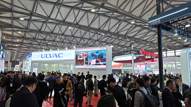
SEMICON China 2026 was held from March 25 to 27, 2026, at the Shanghai New International Expo Centre. During the event, the Hyrnus team explored the latest developments in advanced packaging, semiconductor manufacturing equipment, AI-driven production, and compound semiconductor technologies.
 
Hyrnus team at SEMICON China 2026


Ⅰ. SEMICON China 2026 at a Glance

Held from March 25 to 27 at the Shanghai New International Expo Centre, SEMICON China 2026 covered more than 100,000 square meters and brought together around 1,500 exhibiting companies across more than 5,000 booths. The official post-show report recorded 200,068 cumulative attendee entries, including 142,281 visitor entries and 57,787 exhibitor entries.
The exhibition covered the extended electronics supply chain, including chip design, wafer manufacturing, assembly and packaging, testing, equipment, materials, photovoltaics and display technologies. For equipment suppliers and manufacturers, the scale of the event provided a clear view of where investment and process development are moving next.


Ⅱ. Advanced Packaging Is Moving Toward Broader Production

Advanced packaging and heterogeneous integration were among the most visible topics at SEMICON China 2026. Industry discussions focused on technologies that support AI computing and high-bandwidth data transfer, including 2.5D and 3D integration, Chiplet architectures, HBM, hybrid bonding and co-packaged optics.

These technologies place higher demands on manufacturing equipment. As package structures become denser and more complex, manufacturers require tighter placement and bonding accuracy, more stable process control, better inspection capability and stronger data traceability. The trend is not limited to a single packaging step; it affects die bonding, wire bonding, molding, inspection, testing and material handling throughout the production flow.


Ⅲ. AI Is Changing Semiconductor Manufacturing, Not Only Chip Design

AI was discussed not only as a driver of chip demand, but also as a practical tool for semiconductor production. The Smart Manufacturing Forum and related sessions highlighted the growing role of connected equipment, production data, automated analysis and intelligent process control in the factory of the future.

For semiconductor equipment, this means that mechanical performance alone is no longer enough. Manufacturers increasingly expect machines to support recipe management, process monitoring, alarm records, MES connectivity and data-based quality analysis. Predictive maintenance and closed-loop process optimization are also becoming more important as factories work to improve yield and reduce unplanned downtime.


Ⅳ. Wafer Processing, Materials and Compound Semiconductors Remain Critical

The event also featured dedicated discussions on wafer processes and equipment, advanced materials, and compound semiconductor technologies. Sessions covered SiC, GaN and III-V materials and devices, reflecting continued demand from power electronics, automotive, communications and AI infrastructure applications.

These developments create opportunities across both front-end and back-end manufacturing. New substrates, materials and device structures often require changes in cleaning, bonding, dispensing, thermal processing, inspection and testing. Equipment flexibility and process compatibility will therefore remain important for manufacturers serving multiple device types and packaging formats.


Ⅴ. What the Hyrnus Team Took Away from the Exhibition

Through on-site visits and technical exchanges, the Hyrnus team gained a more direct understanding of current equipment requirements and customer priorities. Three points were especially clear:
  • Precision and stability remain fundamental. Higher-density packaging requires accurate motion control, repeatable bonding and consistent process results.
  • Equipment integration is becoming essential. Customers increasingly need machines that can exchange data with MES systems and support traceable production.
  • Flexible solutions have greater long-term value. Equipment must adapt to changing package types, materials, production volumes and process requirements.


Ⅵ. Continuing to Support Semiconductor Manufacturing Projects

SEMICON China 2026 showed that semiconductor manufacturing is moving toward greater integration, intelligence and process control. Advanced packaging, AI-enabled factories and new semiconductor materials will continue to raise the requirements placed on production equipment.

Hyrnus will continue to follow these industry developments and support customers with equipment and process solutions for wafer processing, die bonding, wire bonding, molding, trim and form, inspection and testing, and test handling. Our focus remains on practical equipment configurations, stable production performance and technical support matched to each customer’s application.
 
Explore Hyrnus semiconductor equipment solutions or contact our team to discuss your process and production requirements.


leave a message

leave a message
If you are interested in our products and want to know more details,please leave a message here,we will reply you as soon as we can.
Contact us:allen@hyrnus.com