Enter product details (such as color, size, materials etc.) and other specific requirements to receive an accurate quote.
leave a message
If you are interested in our products and want to know more details,please leave a message here,we will reply you as soon as we can.

other
TO-247 Power Device Packaging: Complete Process Solution for High-Power Applications

TO-247 Power Device Packaging: Complete Process Solution for High-Power Applications

June 15, 2026
Introduction
The global discrete TO package market reached $4.83 billion in 2025, growing 8.1% year-over-year, driven by the surging demand for power devices in new energy vehicles, photovoltaic inverters, and energy storage systems. Among all TO package families, TO-247 stands out as the premier choice for high-power, high-current applications—capable of handling 30–80A with 3 to 5 pins, making it the go-to package for IGBTs, SiC MOSFETs, and super-junction MOSFETs in industrial drives, EV traction inverters, on-board chargers, and DC-DC converters.
As SiC MOSFET devices increasingly adopt TO-247 packaging for its excellent heat dissipation performance—enabling rapid heat dissipation and stable operation in high-temperature environments—the demand for reliable, high-quality TO-247 packaging solutions has never been greater.
 
This article provides a comprehensive overview of the complete TO-247 packaging process, covering every step from wafer preparation to final test, with recommended equipment solutions for each stage.


Overview
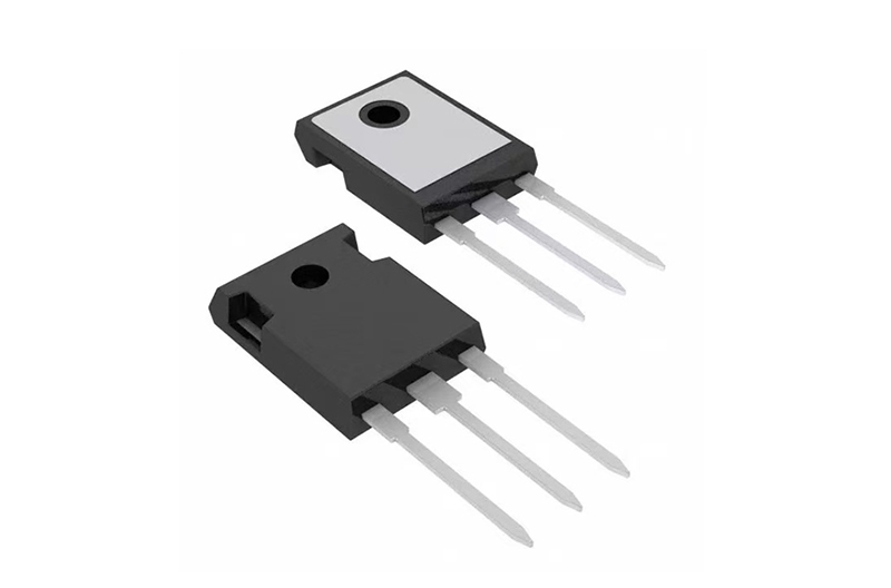
TO-247 is a through-hole power package characterized by:
  • Large die size: Accommodates the largest power chips in the TO family
  • 3–5 pins: Standard 3-pin (TO-247-3L), 4-pin with Kelvin emitter (TO-247-4L), and 5-pin variants
  • Integrated heat sink tab: The backside metal tab serves as both thermal and electrical connection
  • Current capacity: 30–80A, with some variants supporting up to 200A
  • Ultra-thick aluminum wire bonding: 300–500μm aluminum wires, often multi-wire parallel connections to reduce resistance and enhance current-carrying capability
 
 TO-247 package
 
Complete TO-247 Packaging Process Flow
The TO-247 packaging process follows the standard TO-series workflow with specific adaptations for high-power requirements:
Wafer Backgrinding → Wafer Dicing → Plasma Cleaning → Die Attach → Wire Bonding → Molding → Trim & Form → Test & Sort → Inspection
Below is a detailed breakdown of each step with recommended equipment.
 
Step 1: Wafer Backgrinding (Wafer Thinning)
Power device chips for TO-247 are typically 200–350μm thick with backside metallization for optimal heat dissipation. The wafer must be ground to the target thickness while maintaining surface quality for subsequent die attach.
Recommended Equipment Item Purpose
Fully Automatic Grinding/Polishing Machine HY-TP9730 Power chip backside thinning + polishing, reducing thermal resistance
 
 
Step 2: Wafer Dicing
TO-247 features large die sizes with wide scribe lines. Dicing must prevent chipping and cracking, as power chips are more susceptible to mechanical damage during singulation.
Recommended Equipment Item Purpose
Fully Automatic Dual-Spindle Dicing Saw + Sorter HY-WD1202 Large power chip singulation, crack and chipping prevention


Step 3: Plasma Cleaning
The copper or iron-nickel leadframe, along with the chip surface, must be thoroughly cleaned of oils, oxides, and particles. This step is critical for preventing delamination during molding and ensuring strong die attach and wire bond adhesion.
Recommended Equipment Item Purpose
Vacuum Plasma Cleaner HY-EI160 Large-area leadframe batch cleaning, delamination prevention


Step 4: Die Attach
TO-247 requires high-power die attach with silver epoxy or eutectic bonding. The large island area demands high placement force and precision, with die shear strength ≥5kg. For SiC/GaN devices, eutectic die attach is preferred for superior thermal conductivity and high-temperature reliability.
Recommended Equipment Item Purpose
High-Power Die Bonder HY-DB812 TO-247 large-power die attach, high shear strength, high thermal conductivity
Eutectic Die Bonder HY-GD4000 High-power SiC/GaN device eutectic attach


Step 5: Wire Bonding (Critical for Power Devices)
Wire bonding is arguably the most critical step in TO-247 packaging. Unlike small-signal devices, TO-247 demands ultra-thick aluminum wire bonding (300–500μm) with multiple parallel wires to handle high currents while minimizing resistance and inductance. The large die and thick wires require specialized deep-access bonders with high ultrasonic power.
Recommended Equipment Item Purpose
Dual-Head Heavy Aluminum Wire Bonder HY-HW3850 TO-247 high-current thick aluminum wire bonding, resistance reduction, current capacity enhancement


Step 6: Molding (Transfer Molding)
TO-247 requires large molds with high clamping pressure (up to 180 tons) due to the large package size and thick epoxy resin encapsulation. The molding process must minimize voids and ensure complete fill around thick bond wires and large chips.
Recommended Equipment Item Purpose
Fully Automatic Molding System (180T) HY-PS8180 TO-247 high-pressure large-mold molding, void reduction, heat dissipation optimization


Step 7: Trim & Form
After molding, the leadframe must be trimmed and formed. TO-247 features a long frame with 3–5 thick pins requiring robust trimming and forming capabilities. Coplanarity must be controlled to ≤0.1mm.
Recommended Equipment Item Purpose
Fully Automatic Trim & Form System HY-TF221 TO-247 dedicated trimming, bending, and singulation


Step 8: Test & Sort
TO-247 requires high-voltage, high-current testing with temperature control and forced air cooling. The test socket must handle heavy devices and prevent pin burn-out during high-current testing.
Recommended Equipment Item Purpose
Heavy-Duty Turret Handler HY-TS936H TO-247 high-voltage, high-current testing, burn-out prevention, high-volume production


Step 9: AOI & X-Ray Inspection
For TO-247, X-Ray inspection is mandatory to check internal voids, wire sweep, and chip shift. AOI inspection verifies external package quality and pin integrity.
Recommended Equipment Item Purpose
X-Ray Inspection System HY-XR5010 Void detection, broken wire inspection, chip shift detection
AOI System HY-BI300 Package appearance, pin deformation inspection


Summary
TO-247 packaging represents the pinnacle of through-hole power device packaging, offering unmatched current-handling capability, excellent thermal performance, and proven reliability for the most demanding high-power applications. The complete packaging process—from wafer backgrinding through final inspection—requires specialized equipment at every stage, particularly for:
  • Ultra-thick aluminum wire bonding (300–500μm) with multi-wire parallel configurations
  • High-pressure molding (180T) with large, dedicated molds
  • Heavy-duty testing with temperature control and forced air cooling
  • X-Ray inspection for internal void and wire integrity verification


For more information on TO-247 packaging equipment and solutions, contact our technical sales team.

leave a message

leave a message
If you are interested in our products and want to know more details,please leave a message here,we will reply you as soon as we can.
Contact us:allen@hyrnus.com