Enter product details (such as color, size, materials etc.) and other specific requirements to receive an accurate quote.
leave a message
If you are interested in our products and want to know more details,please leave a message here,we will reply you as soon as we can.

other
DIP-8 Package Solution: Full Process Flow, Equipment, and Quality Control for Dual In-Line Packaging

DIP-8 Package Solution: Full Process Flow, Equipment, and Quality Control for Dual In-Line Packaging

June 10, 2026
Overview
The DIP-8 (Dual In-line Package) remains one of the most widely used through-hole semiconductor packages for industrial, power management, automotive, instrumentation, and legacy electronic applications. Thanks to its mature manufacturing process, excellent mechanical reliability, and low production cost, DIP-8 continues to be a practical choice for many analog and mixed-signal devices.
This guide explains the package features, common applications, manufacturing process, and recommended equipment while introducing a complete production solution.


What Is a DIP-8 Package?
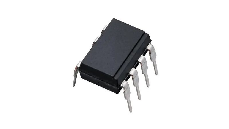
DIP-8 is a standard through-hole package with eight leads arranged in two parallel rows at a 2.54 mm pitch. It is easy to assemble, inspect, replace, and repair, making it suitable for prototyping and high-reliability products.
 
 DIP-8 package
Key Features
DIP (Dual In-line Package) is one of the longest-lived package forms in semiconductor history. As the standardised model of the series, DIP-8 offers the following key advantages:
  • Through-hole package for reliable PCB assembly.
  • Better heat dissipation than many compact SMT packages.
  • Mature and cost-effective manufacturing.
  • High mechanical strength.
  • Standardized dimensions and broad component compatibility.


Typical Applications
  • Operational amplifiers
  • Voltage comparators
  • Timer ICs
  • EEPROMs
  • Interface ICs
  • Optocouplers
  • Power management ICs
  • Industrial control electronics
  • Automotive electronics
  • Consumer products.


Full Manufacturing Process for DIP-8
DIP-8 follows the unified DIP process flow. The complete process chain is detailed below.
 
Step 1 : Wafer Preparation
Objective : Thin the raw wafer to packaging thickness, remove edge stress, and obtain a flat surface.
Sub-steps : Grinding → Edge rounding → Polishing → Wax mounting
Key Control Parameters :
  • Final thickness : 150–200 μm
  • TTV (Total Thickness Variation) :  ≤ ±5 μm
  • Surface roughness (Ra) :  ≤ 0.05 μm
  • Edge chipping : ≤ 50 μm
 
Step 2 : Wafer Dicing (Sawing)
Objective : Separate the whole wafer into individual dies.
Method : Mechanical diamond blade dicing.
Key Control Parameters :
  • Kerf width : 30–60 μm
  • Chipping size : ≤ 5 μm
  • Die size tolerance : ± 25 μm
  • Cut depth Wafer thickness : + 10–20 μm
 
Step 3 : Plasma Cleaning
Objective : Remove contaminants and oxides from die and leadframe surfaces, activate surface energy to improve die attach and wire bond adhesion.
Process Gas : O₂/Ar mixed plasma.
Key Control Parameters :
  • Cleaning time : 60–180 s
  • RF power : 100–300 W
  • Gas flow (O₂) : 50–200 sccm
 
Step 4 : Die Attach
Objective : Precisely attach the die to the leadframe die pad using adhesive.
Method : Silver epoxy dispensing → die pick-and-place → step-cure baking
Key Control Parameters :
  • Placement accuracy (XY) : ± 25 μm
  • Adhesive layer thickness : 20–50 μm
  • Cure temperature profile : 120°C → 150°C (step)
  • Die shear strength : ≥ 2.5 kg
 
Step 5 : Wire Bonding
Objective : Create electrical interconnections between die pads and inner leadframe fingers using metal wires.
Method : Ultrasonic thermocompression ball bonding (gold or copper wire).
Key Control Parameters :
  • Wire pull strength (25 μm Au) : ≥ 5 gf
  • 1st bond ball diameter : 45–55 μm
  • 2nd bond stitch diameter : 60–80 μm
  • Loop height : ≤ 150 μm
 
Step 6 : Moulding (Transfer Molding)
Objective : Encapsulate the die and bond wires with epoxy moulding compound to form the protective body.
Method : Transfer moulding.
Key Control Parameters :
  • Mould temperature : 175°C ± 5°C
  • Clamping pressure : 80–120 T
  • Cure time : 60–120 s
  • Void rate in mould body : ≤ 1%


Step 7 : Trim & Form

Objective : Cut off the tie-bars and form the pins into the standard DIP configuration.
Key Control Parameters :
  • Pin coplanarity : ≤ 0.1 mm
  • Pin pitch 2.54 mm : ± 0.05 mm
  • Pin perpendicularity : ≤ 2°


Step 8 : Test & Sort

Objective : Perform electrical parameter tests and automatically sort good parts from defective ones.
Test Items : Open/short test, functional test, DC parametric test, temperature-characteristic sample test.
 
Step 9 : Visual / Quality Inspection
Objective: Comprehensive inspection of appearance, internal structure, and process reliability.
Inspection Methods :
  • AOI : mould surface defects, pin deformation, marking clarity
  • X-Ray (sampling) : internal voids, wire sweep, die placement
  • Pull-shear test (sampling) : wire pull strength, die shear strength
  
 
DIP-8 Production Line Equipment Configuration Summary
Process Step Recommended Equipment
Wafer Grinding HY-AT9530 Automatic Grinder
Edge Rounding HY-WC615 Edge Rounder
Polishing HY-SP910 Polisher
Wax Mounting HY-SW360 Wax Mounter
Wafer Dicing HY-WD1202 Dual-Spindle Dicing Saw
Plasma Cleaning HY-EI160 Vacuum Cleaner
Die Attach HY-DD560P Automatic Dispensing & Die Bonder
Wire Bonding HY-WB200 Automatic Wire Bonder
Moulding HY-PS8120 Molding System
Trim & Form HY-TF200L Automatic Trim
Test & Sort HY-TT1801 Test & Taping Integrated Machine
AOI Inspection HY-BI300 Appearance Inspection Machine
X-Ray Inspection HY-XR5010 X-RAY Inspection Equipment
Pull-Shear Test HY-PT8100 Push-Pull Force Tester
*Equipment compatibility note: Except for moulding, trim/form, and die attach tools that require dedicated change-kits, all frontend (grinding/dicing/cleaning) and back-end (test/inspection) equipment can be shared across the entire DIP family (6–40 pins), offering high line flexibility for future expansion.


Why Choose HYRNUS

HYRNUS provides complete semiconductor packaging solutions covering wafer preparation, die bonding, wire bonding, molding, trim & form, testing, and inspection. Our turnkey solutions help customers improve production efficiency, ensure consistent quality, and build scalable DIP packaging lines with global technical support.


Summary and Recommendations

DIP-8 remains a proven semiconductor package thanks to its standardized design, reliable performance, and economical manufacturing process. By combining optimized production processes with suitable equipment and strict quality control, manufacturers can achieve stable, high-yield production. HYRNUS offers complete equipment solutions for every stage of the DIP-8 packaging process.Contact us for a tailored DIP-8 equipment configuration.


FAQs

What is the a DIP-8 package?
The DIP‑8 (Dual In‑line Package, 8‑pin) is one of the most classic standard package forms in semiconductor assembly.
What are the main application fields for DIP-8?
Op‑amps , comparators , timers , regulators , EEPROMs, optocouplers, and driver ICs. Used in consumer, industrial, automotive, communication, medical, and maker boards.
Differences from other DIPs?
DIP‑14/16 are longer but still narrow body, use same 120T. DIP‑28/40 are wide body and need 180T and heavy‑duty trim. Process is identical.
Is DIP-8 outdated?
No. Still essential for industrial/automotive (long life), prototyping/breadboards, and high‑power/voltage applications due to reliability and cost.


leave a message

leave a message
If you are interested in our products and want to know more details,please leave a message here,we will reply you as soon as we can.
Contact us:allen@hyrnus.com