Die Attach vs. Wire Bonding: What Is the Difference?

Die attach and wire bonding perform two different but closely related functions in conventional semiconductor packaging. Die attach secures the semiconductor die to a lead frame, substrate, package base, or heat spreader. Wire bonding then creates electrical connections between the die pads and the package leads or substrate traces. In simple terms, die attach provides the physical foundation, while wire bonding provides the electrical pathway.
Understanding the difference is important when evaluating packaging processes, diagnosing assembly defects, or selecting die bonding and wire bonding equipment. This article compares their functions, materials, process sequence, quality indicators, and equipment requirements.
1. What Is Die Attach?
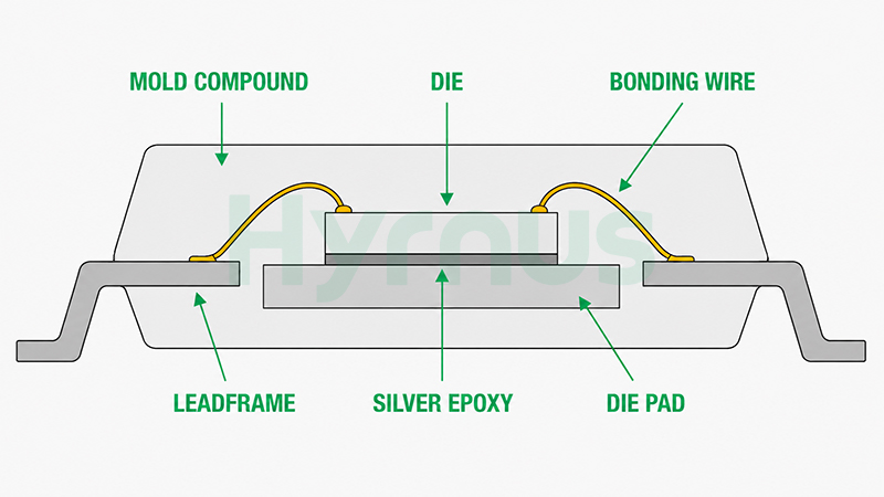
Die attach, also called die bonding or die mounting, is the process of accurately placing and bonding a separated semiconductor die onto a carrier. Depending on the package design, the carrier may be a lead frame, ceramic or organic substrate, package base, or heat sink.
In a conventional face-up wire-bonded package, die attach is normally completed before wire bonding. The selected attachment material and process must hold the die in position while also meeting the thermal, electrical, and reliability requirements of the device.
Main Functions of Die Attach
- Mechanical support. The bond layer prevents the die from shifting, tilting, lifting, or separating during later operations such as curing, wire bonding, molding, and testing.
- Thermal management. The attachment layer can provide a heat-transfer path from the die to the package structure, which is especially important for power devices and other heat-generating components.
- Electrical connection when required. Conductive epoxy, solder, eutectic alloys, and sintered materials may provide grounding or current conduction through the backside of the die, depending on the device design.
Common Die Attach Methods
- Epoxy or silver-filled epoxy bonding
- Eutectic bonding, including AuSn processes
- Soft-solder die bonding
- Pressure-assisted or pressureless sintering for selected power-device applications
Typical Die Attach Equipment
Die attach equipment may include automatic die bonders, eutectic die bonders, adhesive dispensing systems, solder die attach systems, and sintering systems. Important selection factors include placement accuracy, die size and thickness, bonding material, temperature and force control, substrate handling, vision alignment, and required production capacity.
2. What Is Wire Bonding?
Wire bonding is an interconnection process that uses fine metal wire or ribbon to connect bond pads on the die to leads or conductive traces on the package substrate. These connections carry power and electrical signals between the semiconductor die and the external circuit.
In many conventional packages, wire bonding follows die attach after the die has been secured and any required curing, reflow, cleaning, or surface-preparation steps have been completed.
Main Functions of Wire Bonding
- Electrical interconnection. Wire bonds create conductive paths for power, ground, and signal transmission.
- Controlled loop formation. The wire loop must maintain the required height, length, clearance, and geometry without contacting nearby wires, package surfaces, or encapsulation features.
- Reliable metallurgical bonding. The first and second bonds must achieve sufficient strength and consistency while avoiding pad damage, cratering, excessive deformation, or wire breakage.
Common Wire Materials and Bonding Types
- Gold and copper wire are widely used in ball bonding applications.
- Aluminum wire and ribbon are commonly used in wedge bonding.
- Heavy aluminum or copper wire and ribbon are used for power semiconductor modules and high-current devices.
Typical Wire Bonding Equipment
Wire Bonding equipment includes automatic ball bonders, wedge bonders, deep-access wire bonders, and heavy-wire or ribbon bonders. Key selection factors include wire material and diameter, pad pitch, bond area, package depth, loop requirements, ultrasonic and force control, vision capability, throughput, and process-monitoring functions.
3. Where Do Die Attach and Wire Bonding Fit in the Packaging Process?
A simplified process flow for a conventional wire-bonded IC package is:
Wafer Back Grinding → Wafer Dicing → Die Attach → Cure / Reflow / Sintering → Surface Preparation as Required → Wire Bonding → Molding or Encapsulation → Trim and Form → Final Test and Sorting
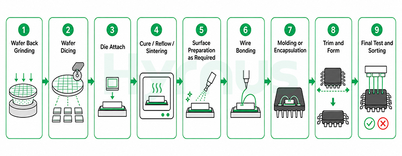
*The exact sequence varies by package architecture, materials, and production requirements. Flip-chip, clip-attach, wafer-level, and other advanced packaging structures may use different interconnection flows.
4. Key Differences Between Die Attach and Wire Bonding
| Comparison Item | Die Attach | Wire Bonding |
| Process position | Usually before wire bonding in a conventional package | Usually after die attach and required intermediate steps |
| Primary purpose | Secure the die and support thermal or electrical requirements | Connect die pads to package leads or substrate traces |
| Main interface | Backside or bonding surface of the die to the carrier | Top-side bond pads to external connection points |
| Common materials | Epoxy, silver epoxy, solder, eutectic alloy, sintered material | Gold, copper, aluminum wire, or ribbon |
| Key quality indicators | Placement accuracy, die tilt, bond-line thickness, voiding, adhesion or shear strength | Bond strength, deformation, loop geometry, continuity, pull or shear results |
| Common defects | Die shift, die tilt, insufficient adhesion, overflow, contamination, voids | Non-stick bonds, weak bonds, lifted bonds, broken wire, shorting, open circuit, poor loop shape |
| Typical equipment | Die bonder, eutectic bonder, dispenser, solder or sintering system | Ball bonder, wedge bonder, deep-access bonder, heavy-wire bonder |
5. How Can Die Attach Quality Affect Wire Bonding?
Although the two processes use different materials and machines, poor die attach can reduce wire-bonding stability. Common interactions include:
- Die shift. Bond pads may no longer match the programmed bonding coordinates, increasing the risk of off-pad bonds or alignment failures.
- Die tilt or uneven bond-line thickness. Changes in die height and planarity can affect focus, bond force consistency, loop height, and tool clearance.
- Insufficient attachment strength. The die may move under bonding force or ultrasonic energy, resulting in unstable or weak bonds.
- Adhesive overflow or surface contamination. Contamination near the pad area can prevent proper metallurgical bonding and cause non-stick or lifted bonds.
- Excessive voiding or warpage. These conditions may weaken thermal or mechanical stability and indirectly narrow the wire-bonding process window.
For this reason, die position, planarity, adhesion, cleanliness, and cure condition should be verified before wire bonding begins. Stable upstream control reduces the amount of compensation required at the wire-bonding stage.
6. Conclusion
The main difference between die attach and wire bonding is straightforward: die attach secures the semiconductor die, while wire bonding connects it electrically to the package. However, reliable packaging depends on more than completing the two steps in the correct order. Placement accuracy, material compatibility, surface cleanliness, bond strength, loop control, thermal behavior, and equipment stability all influence final yield and device reliability.
HYRNUS provides die bonding equipment and wire bonding equipment for semiconductor packaging, optoelectronic devices, power devices, MEMS, hybrid circuits, and related assembly applications. For a new package or production process, contact our engineering team with your die, substrate, material, accuracy, and capacity requirements to evaluate a suitable equipment configuration.
FAQ
Is die attach the same as die bonding?
In most semiconductor assembly contexts, the terms are used interchangeably. “Die attach” emphasizes the process, while “die bonder” commonly refers to the equipment used to place and bond the die.
Does wire bonding always come immediately after die attach?
Not necessarily. A curing, reflow, sintering, plasma cleaning, or inspection step may be required between them. However, the die must be securely attached before conventional face-up wire bonding can be performed.
Can wire bonding replace die attach?
No. They serve different functions in a conventional wire-bonded package. Alternative architectures such as flip chip or copper clip interconnect may replace wire bonds or combine attachment and electrical interconnection differently.
What information is needed before selecting equipment?
Provide the die and substrate dimensions, package structure, bonding materials, target accuracy, wire or ribbon specification, process temperature and force requirements, expected capacity, and automation level.