What Are You Looking For?


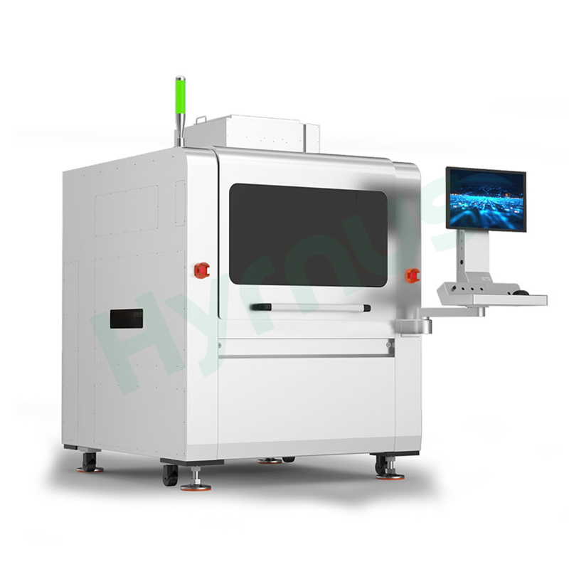
HY-BI300P Aoi Machine is equiped with Post Semiconductor Packaging 2D+3D Full Dimension Quality Control Equipment covers all defects in wire bonding (gold wire / aluminum wire bonding) and chip appearance.
Brand :
HYRNUSItem No. :
HY-BI300POrder(MOQ) :
1 SetWarranty :
One-Year Warranty and Lifetime MaintenancePayment :
T/TLead Time :
7-35 DaysProduct Origin :
ChinaHigh Performance Wire Bonding & Chip Appearance Inspection Machine
 Product Introduction
HY-BI300P Wire Bonding & Chip Appearance Inspection Machine is suitable for automotive electronics, industrial grade, consumer electronics and other scenarios, realizing 100% full inspection and data traceability, helping packaging and testing plants improve yield, reduce costs and enhance efficiency.
Application Scenarios
High-end 3D configuration for high-end / complex product lines: Dual cameras are adopted to separately deliver high-precision 2D inspection and high-speed 3D inspection
Suitable for production lines with large-size carriers, deep cavities, and stricter requirements for wire loop height and gold ball morphology, such as high-end Memory, TR devices, power devices, etc
Key Algorithm & Performance Features
Point cloud algorithms overcome imaging challenges in scenarios with crossed wires and large depth of field. The 2D+3D dual mode inspection allows 2D to cover full appearance defects, while 3D accurately measures wire loop height to meet strict inspection standards for high end products.With multi layer image acquisition and wire width percentage based defect judgment, the system unblocks the data link and forms a full process closed loop management of “real time inspection – precise analysis – process optimization”.
RGB Multi-Channel Light Source
Multi-Channel Fusion Technology
Gold Wire Extraction Algorithm
High-Speed Flying Capture
Ultra-Deep Focus Synthesis
High-Precision 3D Inspection
AI-Assisted Programming
Inspection Result Re-Judgment
Product Features
Cross-wire short circuit, abnormal wire loop, broken wire, gold / aluminum ball offset, cold joint, uneven wire diameter
Surface scratches, chipping, foreign particles, adhesive residue, cracks, poor marking
Pad oxidation, contamination, dimensional deviation
Solves single-layer cross-wire inspection issues
Supports multi-layer algorithms and wire width percentage defect detection
Significantly outperforms traditional 3D line-scan technology in precision and frame rate
Supports standalone offline or in-line production
Self-developed point cloud algorithm + ultra-depth-of-field fusion technology for wire bond and die appearance inspection in cross-wire and ultra-large depth-of-field scenarios
Portable and user-friendly interface with guided programming
Key Specifications
| Item | Specification |
| Pixel Resolution | 3.2 μm |
| 2D Inspection Accuracy | ±2 μm |
| Full Inspection | 100% |
| Loop Height Measurement | ±10 μm |
| 2D Pixel Resolution | 2.5 μm |
| 2D Field of View (FOV) | 10 mm × 10 mm |
| 3D Pixel Resolution | 3.2 μm |
| 3D Field of View (FOV) | 22 mm × 22 mm |
| Depth of Field | 200 μm |
| Compatible Product Dimensions | 50~300 mm (L) × 50~300 mm (W) × 0.1~30 mm (H) |
Parameter Specifications
| Item | Parameter |
| Equipment Name | Wire Bond & Die Visual Inspection Machine |
| Model | HY-BI300P |
| 2D/3D Accuracy | 2D: 2.5 µm |
| 3D: 3.2 µm | |
| Field of View | 2D: 10 mm × 10 mm |
| 3D: 22 mm × 22 mm | |
| Detectable Solder Joint Defects | Defect width ≥ 3 Pixel, contrast ≥ 30 bit:No bond, bond offset, bond size, bond thickness, golf ball defect |
| Detectable Wire Defects | Defect width ≥ 3 Pixel, contrast ≥ 30 bit:Mis-wire, missing wire, broken wire, wire offset (snaking), re-bond, wire sag (horizontal), bridged wire, extra tail, wire sag (vertical), wire loop height, cross-wire spacing |
| Detectable Die Defects | Defect width ≥ 3 Pixel, contrast ≥ 30 bit:Die chipping, die rotation, die missing, die crack, ink spot, die offset, scratch, foreign material contamination, epoxy coverage, die tilt |
| Substrate Size | 50~300 mm (L) × 50~300 mm (W) × 0.1~30 mm (H) |
| Equipment Dimensions | 1400 × 1550 × 1750 mm |
| Weight | 1500 kg ± 5% |
| Power Rating | 2.5 kW |
Inspection Items
| Wire Breakage | Missing Bond | Scratches | Misalignment / Angular Deviation |
| Wire Bundling | Bond Pad Misalignment | Cracking | Silver Glue/Epoxy Overflow |
| Wire Collapse | Abnormal Ball Diameter | Oxidation | Chipping |
| Abnormal Wire Arc | Chip Appearance Defects | Contamination | Missing Chip |
Product Details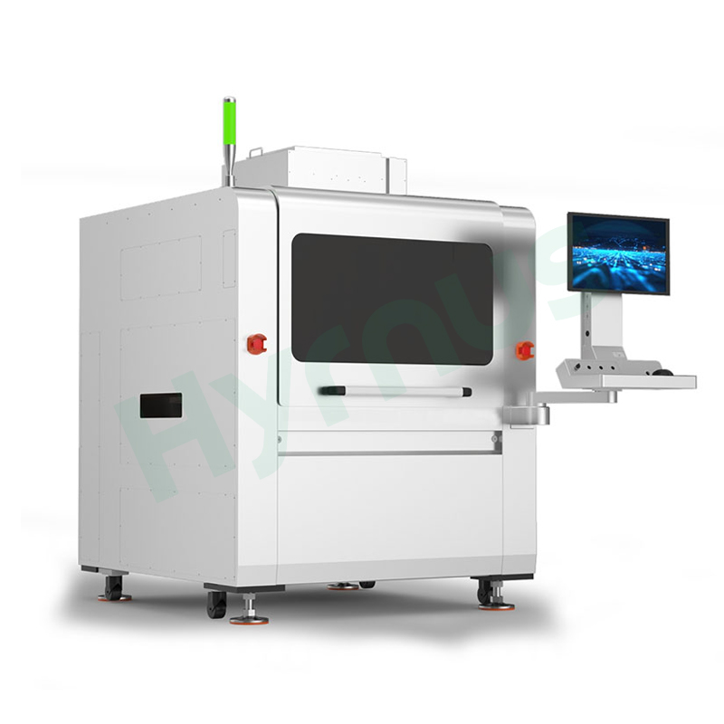
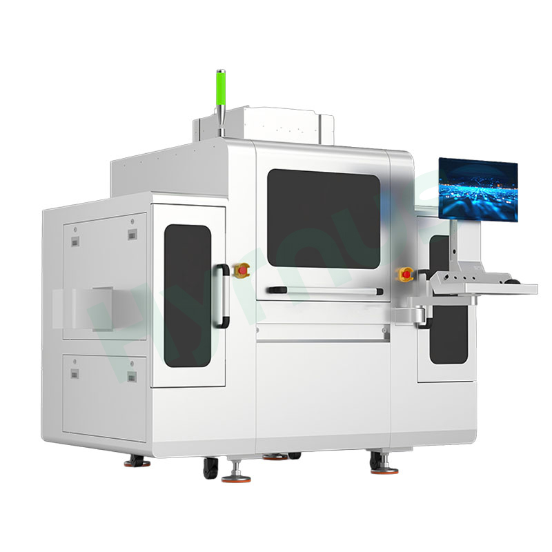
HY-BI300R Aoi Test is an advanced 2D+3D integrated AOI inspection platform designed for high-end semiconductor packaging applications, combining wire bond and die surface inspection with height-sensitive 3D measurement capabilities.
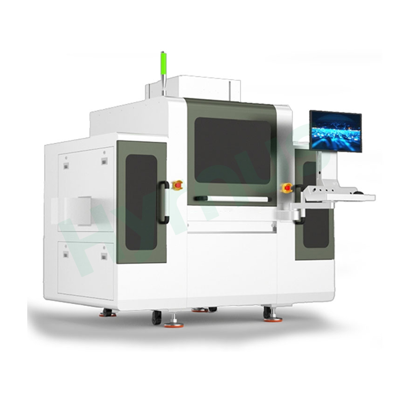
HY-BI300 Aoi Equipment is a fully automatic 2D AOI inspection system engineered for semiconductor back-end quality assurance, addressing wire bonding and die surface defects across SIP, COB, IC, power devices, optical communication, and LED packaging applications.
leave a message
Scan To Wechat :

Scan To WhatsApp :