Enter product details (such as color, size, materials etc.) and other specific requirements to receive an accurate quote.
leave a message
If you are interested in our products and want to know more details,please leave a message here,we will reply you as soon as we can.

other
TO252 (DPAK) Power Semiconductor Packaging Line Solution

TO252 (DPAK) Power Semiconductor Packaging Line Solution

June 10, 2026
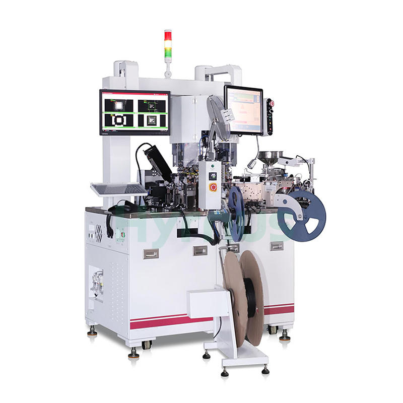
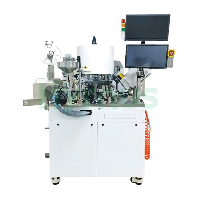
HYRNUS provides TO252 (DPAK) packaging equipment and production line solutions for MOSFETs, Schottky diodes, rectifiers, TVS devices, and other power semiconductor products.
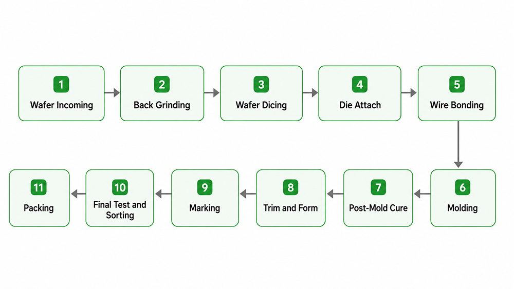
Based on the die size, lead frame design, die attach material, wire bonding method, package structure, electrical test requirements, and target throughput, we can configure stand-alone machines, semi-automatic lines, or fully automated packaging and testing lines. The process scope can cover wafer back grinding, wafer dicing, die attach, wire bonding, molding, post-mold curing, trim and form, marking, final testing, sorting, and packing.


What Is a TO252 Package?
 
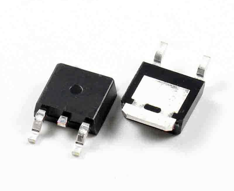
TO252, also known as DPAK, is a surface-mount package widely used for power semiconductor devices. Its compact body is compatible with SMT assembly, while the exposed metal tab and lead frame provide an efficient thermal path from the semiconductor die to the printed circuit board.
Compared with larger through-hole power packages, TO252 is better suited to automated assembly and space-efficient PCB design. It is commonly selected for high-volume applications in consumer electronics, automotive electronics, industrial power supplies, and new energy systems.
 
 
Key Benefits of the TO252 Package
Feature Production and Product Benefit
SMT Compatibility Supports automated placement and reflow assembly.
Compact Size Reduces PCB space requirements and supports higher component density.
Good Thermal Performance Provides an effective heat transfer path through the lead frame and mounting pad.
Cost Efficiency Suitable for high-volume manufacturing with a relatively economical package structure.
High Automation Potential Can be processed through continuous die attach, wire bonding, molding, forming, and test operations.
Application Reliability Can be engineered for consumer, industrial, and automotive-grade power applications.
 
 
Typical Applications
Application Area Typical Products
Consumer Electronics PD fast chargers, adapters, and smart home power modules
Power Management Switching power supplies, DC/DC converters, and LED drivers
Automotive Electronics Battery management systems, ECUs, motor drives, and onboard power modules
Industrial Control Industrial power supplies, control modules, and drive systems
New Energy Energy storage systems and auxiliary power supplies for photovoltaic inverters
Power Equipment UPS systems and other power conversion equipment


Main Components of a TO252 Device
 
1. Lead Frame
The lead frame is typically made from a copper alloy. It provides electrical connections, a thermal path, and mechanical support. Its dimensional accuracy, surface condition, plating quality, and die pad flatness influence die attach, wire bonding, molding, and final forming quality.
2. Semiconductor Die
The semiconductor die performs the switching, rectification, or power control function. Wafer thickness, dicing quality, die surface condition, and back-side metallization can affect die attach quality, thermal resistance, and long-term reliability.
3. Bond Wire
Bond wire creates the electrical connection between the die pads and the lead frame. Aluminum wire, heavy aluminum wire, ribbon, or another interconnection method may be selected according to current capacity, pad design, loop geometry, and reliability requirements.
4. Molding Compound
The molding compound provides electrical insulation, moisture resistance, and mechanical protection for the die and internal interconnections. Material selection and molding parameters must be coordinated to control voids, delamination, wire sweep, flash, and package stress.


Key Challenges in TO252 Packaging
 
1. Die Attach Quality and Thermal Performance
TO252 devices generate heat during operation. The interface between the semiconductor die and lead frame directly affects thermal resistance, electrical performance, and reliability. The process must control die position, tilt, bond-line thickness, void rate, adhesive coverage, solder wetting, and attach strength.
2. Stable Wire Bonding
Power devices require consistent current-carrying capability. The wire bonding process must accurately control bonding position, force, ultrasonic energy, bonding time, wire diameter, and loop geometry. Unstable parameters can cause weak bonds, pad damage, lifted wires, abnormal loops, or increased electrical resistance.
3. Molding Consistency
The molding process must protect the die and wire connections without creating wire sweep, incomplete fill, voids, delamination, excessive flash, or package cracking. The molding machine, mold design, molding compound, transfer conditions, and cure profile must be matched to the device structure.
4. Trim and Form Accuracy
As an SMT package, TO252 requires controlled lead geometry and coplanarity. Trim and form equipment must maintain lead dimensions while minimizing burrs, package stress, lead deformation, and body cracking.
5. Efficient Final Testing and Sorting
High-volume production requires not only accurate electrical testing, but also stable feeding, orientation, contact, binning, and data recording. The test handler must be selected according to the device type, test time, number of bins, temperature requirements, and target UPH.
6. Manufacturing Cost Control
Package cost has a direct effect on device competitiveness. Equipment utilization, line automation, changeover time, yield, consumable use, maintenance requirements, and overall equipment effectiveness should be considered during line planning.


Complete TO252 Packaging Process
 
1. Wafer Incoming Inspection
Incoming wafer inspection confirms the wafer model, dimensions, thickness, visual condition, wafer map, die layout, back-side condition, and process lot information before grinding and dicing.
Key Process Controls
  • Wafer identification and traceability
  • Initial wafer thickness and warpage
  • Die map and street layout
  • Surface and edge condition
  • Back-side metallization or coating status
 
2. Wafer Back Grinding
Wafer back grinding reduces the wafer to the target thickness required for package height, thermal performance, die strength, and downstream handling.
Key Process Controls
  • Final wafer thickness
  • Thickness uniformity
  • Wafer warpage
  • Surface roughness
  • Edge chipping
  • Post-grinding cleaning and handling


3. Wafer Dicing
The dicing saw separates the wafer into individual dies according to the cutting streets. Stable cutting quality is required so that each die matches the lead frame die pad and can be picked and placed reliably.
Key Process Controls
  • Cutting accuracy
  • Die dimension consistency
  • Chipping and crack control
  • Blade and spindle condition
  • Cutting surface cleanliness
  • Wafer map and die tracking


4. Die Attach
The die bonder places the semiconductor die onto the heat-spreading pad of the TO252 lead frame. Conductive epoxy, solder, eutectic bonding, or another qualified attachment method may be used according to the device design and thermal requirements.
Key Process Controls
  • Die position and rotation
  • Die tilt
  • Adhesive or solder volume
  • Bond-line thickness
  • Placement force
  • Heating and cure profile
  • Void rate and attach strength


Recommended equipment
  • wafer grinding equipment

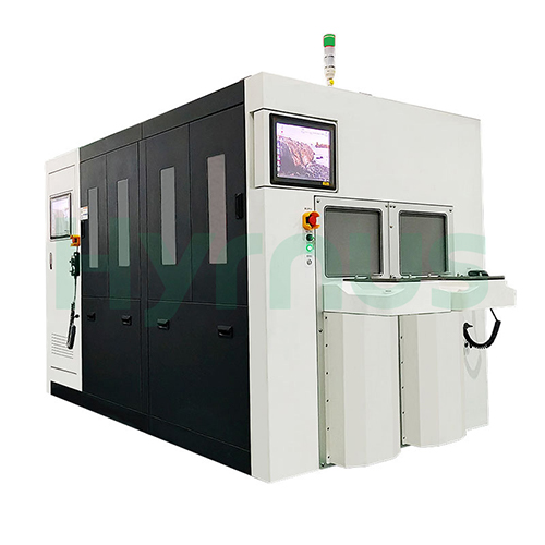
    Wafer Grinder

    HY-WT3005 Fully Automatic Ultra-Precision Wafer Thinning Machine.
  • wafer dicing equipment

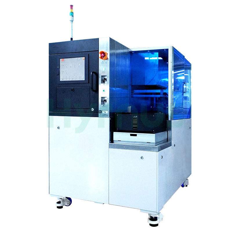
    Dicing Saw

    HY-WD1202 Wafer Singulation Dicing Saw.
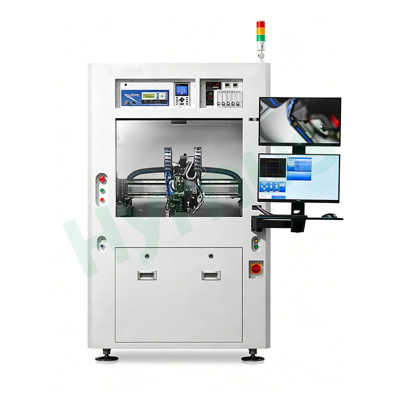
  • die attach machine

    Die Donder

    HY-GD800 Fully Automatic Multi-Function Die Bonder. Typical placement accuracy can reach ±5 μm and ±0.1°, subject to the final product and process configuration.
5. Wire Bonding
Wire bonding creates the electrical connection between the die pads and lead frame. The bonding platform, capillary or wedge, wire material, wire diameter, ultrasonic system, and bonding program must be selected according to the device structure.
Key Process Controls
  • Bonding position
  • Bonding force
  • Ultrasonic energy
  • Bonding time
  • Wire diameter
  • Loop height and span
  • Pull strength and bond quality


6. Molding
Transfer molding encapsulates the die, bond wires, and part of the lead frame with an epoxy molding compound. The process provides insulation, moisture resistance, and mechanical protection.
Key Process Controls
  • Mold temperature
  • Transfer pressure and speed
  • Cavity filling
  • Wire sweep
  • Voids and incomplete fill
  • Flash and bleed
  • Delamination risk
  • Package stress


7. Post-Mold Cure
After molding, post-mold cure completes the cross-linking of the molding compound and stabilizes its mechanical, insulation, and moisture-resistance properties.
Key Process Controls
  • Cure temperature
  • Cure time
  • Loading method
  • Lot separation
  • Oven uniformity
  • Process traceability


8. Trim and Form
Trim and form equipment removes the lead frame tie bars and forms the leads to the required TO252 geometry for SMT mounting
Key Process Controls
  • Lead dimensions
  • Lead coplanarity
  • Forming angle
  • Burr control
  • Package body protection
  • Feeding and strip positioning stability


Recommended equipment

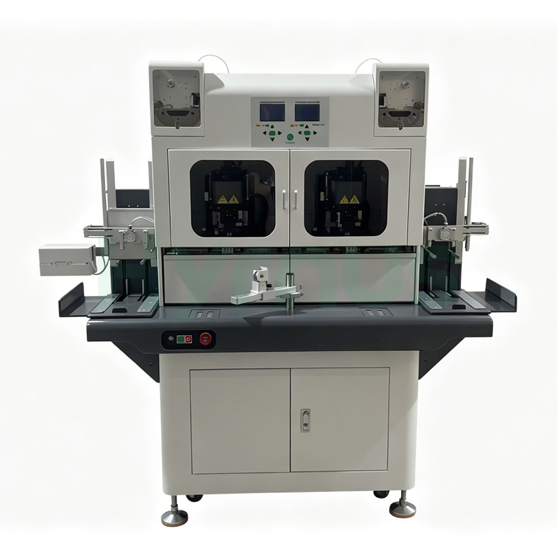
  • ultrasonic wire bonding machine

    Wire Bonding Machine

    HY-HW3850 Automatic Ultrasonic Heavy Aluminum Wire Wedge Bonder
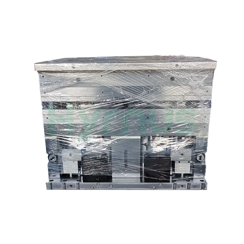
  • molding mold

    Molding Mold

    HY-PM252-6R Molding Mold
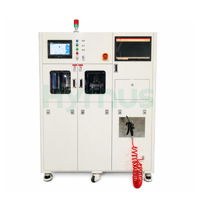
  • trim form machine

    Food Processing & Catering

    HY-TF210 Automatic Trim and Form System


9. Marking and Visual Inspection
The marking system applies product identification and traceability information to the package surface. A vision system can be integrated to verify mark position, content, clarity, and package appearance.
Key Process Controls
  • Product model
  • Batch or lot number
  • Date code
  • Manufacturer information
  • Traceability code
  • Character and appearance inspection


10. Final Test and Sorting
The final test handler feeds, positions, contacts, tests, and sorts finished devices according to the electrical test results.
Key Process Controls
  • Breakdown voltage
  • Leakage current
  • On-resistance
  • Threshold voltage
  • Forward voltage
  • Static electrical parameters
  • Customized device parameters
  • Bin classification and data recording


11. Packing
Qualified TO252 devices are packed according to customer handling and SMT assembly requirements. Packaging specifications should define orientation, quantity, labeling, moisture protection, and traceability.
Key Process Controls
  • Tape-and-reel packing
  • Tube or tray packing where applicable
  • Orientation control
  • Labeling and lot recording
  • Moisture-barrier packaging
  • Final outgoing inspection


  • Test Handle

    HY-TS980 Turret Test Handler
  • ic test handler

    Turret Sorter

    HY-TH800 Turret-Style Integrated System


Recommended Equipment Configuration
 
Process Recommended Configuration Primary Function
Wafer Back Grinding HY-WT3005 Automatic wafer thinning, thickness control, alignment, cleaning, and handling
Wafer Dicing HY-WD1202 Wafer singulation with cutting accuracy and chipping control
Die Attach HY-GD800 Die pickup, vision alignment, adhesive or solder process, and high-precision placement
Wire Bonding HY-HW3850 Electrical interconnection between the die and lead frame
Molding HY-PM252-6R Transfer molding and package encapsulation
Post-Mold Cure Curing Oven Controlled post-mold curing and batch management
Trim and Form HY-TF210 TO252 lead trimming and forming
Marking Automatic Laser Marking System Product identification and traceability marking
Final Test and Sorting HY-TS980 Electrical testing, binning, and automatic device sorting
Packing HY-TH800 Orientation control, counting, packing, and labeling


Flexible Production Line Configurations
 
Stand-Alone Equipment
Suitable for laboratories, process development, pilot production, or replacement and expansion of individual operations in an existing factory.
 
Semi-Automatic Line
Retains selected manual loading or transfer steps while using automatic positioning, processing, inspection, and data recording to improve consistency and reduce labor dependence.
 
Fully Automatic Line
Connects equipment through automatic feeding, material transfer, online inspection, sorting, and production data management to reduce handling between operations and support high-volume manufacturing.
 
Multi-Package Compatibility
Some machines can support TO252, TO220, or other related power packages by changing fixtures, tracks, molds, contact parts, tooling, and process programs. Compatibility must be evaluated against the actual package dimensions, lead frame structure, process parameters, and throughput requirements.


Request a Customized TO252 Packaging Solution

Send us your device drawing, lead frame information, process flow, target capacity, automation requirements, and factory conditions. HYRNUS will evaluate the project and recommend a suitable stand-alone machine configuration or complete TO252 packaging and testing line. 

Contact Our Engineering Team


FAQs

Can the line be customized for different TO252 divices?
Yes. The configuration should be adjusted according to die size, lead frame design, die attach material, bonding method, molding structure, test program, input and output format, and target throughput.
Can individual machines be purchased separately?
Yes. Customers can select a single machine, several connected processes, or a complete packaging and testing line.
Can the equipment also support TO220 products?
Some equipment can support TO220 or related power packages after changing fixtures, molds, tracks, tooling, contact parts, or programs. The final compatibility must be confirmed from the product drawings and process requirements.
Dose HYRNUS provide installation and process support?
Support can include installation, commissioning, trial production, operator training, maintenance training, and ongoing technical assistance, depending on the agreed project scope.


leave a message

leave a message
If you are interested in our products and want to know more details,please leave a message here,we will reply you as soon as we can.
Contact us:allen@hyrnus.com