What Are You Looking For?


HY-XR5010(2.5D) Series performs non-destructive testing for IC packaging, BGA/QFN chips, PCBA and capacitors. Equipped with CNC motion, multi-angle imaging and one-click void analysis, it detects voids, solder faults and dimensional errors. Three models fit small-batch checks, production sampling and lab R&D; optional barcode tracking and a high-res detector spot defects as tiny as 4μm.
Full enclosed lead shielding limits radiation below 1μSv/h, with complete official radiation safety certifications.
Brand :
HYRNUSItem No. :
HY-XR5010(2.5D) SeriesOrder(MOQ) :
1 SetWarranty :
One-Year Warranty and Lifetime MaintenancePayment :
T/TLead Time :
7-35 DaysProduct Origin :
ChinaSemi-Automatic X-RAY Inspection Equipment for Semiconductor IC Packaging and Electronic Capacitors

Product Introduction
HY-XR5010(2.5D) Series Semi-Automatic X-RAY Inspection System is a dedicated non-destructive X-ray inspection system for semiconductor IC packaging, BGA/QFN chips, PCBA and electronic capacitors. With CNC programmable multi-axis motion, multi-angle tilt imaging and one-click automatic void ratio calculation, it accurately detects voids, solder defects and internal dimensional errors. Three configurations (Basic/Standard/Premium) cover small batch quality checks, mass sampling and high-precision lab R&D. Custom barcode scanning function is optional for automatic product information recording to streamline your quality traceability workflow. The built-in high-resolution flat-panel detector delivers clear imaging to spot tiny micro defects down to 4μm.
It adopts full lead radiation shielding with radiation exposure below 1μSv/h and comes with complete official radiation safety certification.
Product Application
◆ Semiconductors
Specialized for IC packaging production lines, performing void rate calculation and hidden solder joint inspection of BGA, QFN and other packaged chips.
◆ Capacitors
Detect internal cavities, cracks and structural defects of various electronic capacitors such as MLCC.
◆ Electronics
Conduct solder void and assembly defect inspection for PCBA circuit boards.
Extended Application (Auxiliary Business)
◆ New Energy
Internal structure and continuity testing of power fuses and energy storage components.
◆ Food
Non-destructive foreign body inspection for packaged food safety control.
Product Functions & Working Principles
This equipment emits X-rays through an X-ray source, which penetrate the interior of the tested object. The receiver receives the X-rays and forms images, based on which personnel manually determine the internal defects of the tested object.
Product Features
1. CNC Programmable Motion
Pre-set motion paths enable automatic multi-point inspection. Ideal for quality evaluation of small-batch products, significantly boosting inspection efficiency.
2. Automatic Void Measurement
One-click automatic calculation to measure the void area ratio of bubbles and cavities inside products.
3. Multi-Angle Inspection
The flat panel supports rotational shooting from 0° to ±60°. Workpieces placed on the carrier stage can rotate freely at any 360° angle.
4. Multi-Layer Safety Protection
The equipment main body adopts lead shielding enclosure, with radiation level lower than the national standard of 1μSv/H. Interlock protection is equipped on the lead door; the X-ray source will shut down automatically once the lead door is opened. The machine has passed radiation safety certification and obtained exemption certificate.
Technical Specifications
| Parameter | Model: HY-XR5010A (2.5D) Basic Version | Model: HY-XR5010A (2.5D) Standard Edition | Model: HY-XR5010A (2.5D) Premium Edition |
| Equipment Performance | |||
| Overall Dimensions | 2200mm (L) × 1400mm (W) × 2000mm (H) | 2200mm (L) × 1400mm (W) × 2000mm (H) | 2200mm (L) × 1400mm (W) × 2000mm (H) |
| Machine Weight | 1800 Kg | 1800 Kg | 2000 Kg |
| Power Supply | 110V/220V/16A | 110V/220V/16A | 110V/220V/20A |
| Power Consumption | 4 kW | 4 kW | 4.6 kW |
| Tilt Angle | ± 60° | ± 60° | ± 60° |
| Stage Rotation | 0° | 0° | 360° |
| Number of Axes | 5 axes | 5 axes | 6 axes |
| Product Entry (Optional) | Manual barcode scanning | Manual / Automatic barcode scanning | Manual / Automatic barcode scanning |
| Inspection Range | Manual 5-sided fluoroscopic inspection | Manual 5-sided fluoroscopic inspection | Automatic 5-sided fluoroscopic inspection |
| Inspection Method | Algorithm-based manual inspection | Algorithm-based manual inspection | Algorithm-based manual inspection |
| Stage Size | 410mm × 460mm | 410mm × 460mm | 410mm × 460mm |
| Max. Stage Load | 6 kg | 6 kg | 5 kg |
| Radiation Level | < 1 μSv/h | < 1 μSv/h | < 1 μSv/h |
| X-Ray Source Performance | |||
| Tube Model | PXS Series | PXS Series | G Series |
| Tube Type | Reflex closed tube | Reflex closed tube | Transmission closed tube |
| Max. Tube Voltage | 110 kV | 110 kV | 100 kV |
| Max. Tube Current | 250 µA | 250 µA | 200 µA |
| Emission Angle | 120° | 120° | 168° |
| Min. Resolution | 7 µm | 7 µm | 4 µm |
| Flat Panel Detector Performance | |||
| Detector Model | Whale Series | NDT Series | MFG Series |
| Detector Type | Amorphous Silicon | New TFT | Amorphous Silicon |
| Resolution | 4.0 Lp/mm | 5.8 Lp/mm | 10 Lp/mm |
| Pixel Size | 125 µm | 85 µm | 49.5 µm |
| Pixel Matrix | 1024 × 1248 | 1536 × 1536 | 2312 × 2904 |
| Effective Imaging Area | 160mm × 128mm | 130mm × 130mm | 114mm × 143mm |
| A/D Conversion Bit Depth | 16 bit | 16 bit | 14 bit |
| Frame Rate (1×1) | 30 fps | 20 fps | 10 fps |
| Features & Applications | Suitable for PCBA void rate and solder joint inspection; fuse continuity/discontinuity inspection in new energy and capacitor industries. This model is mainly used for internal structure and process effect inspection. | Mainly used for internal structure and dimensional inspection, with product accuracy up to 0.01mm. Widely used as high-precision measurement equipment in PCBA and new energy fields. | Multi-angle automatic fluoroscopic inspection, suitable for complex-structured products requiring high precision. Used in R&D laboratories, sampling inspection, and high-precision spot check processes. |
Product Details
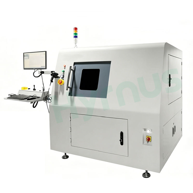
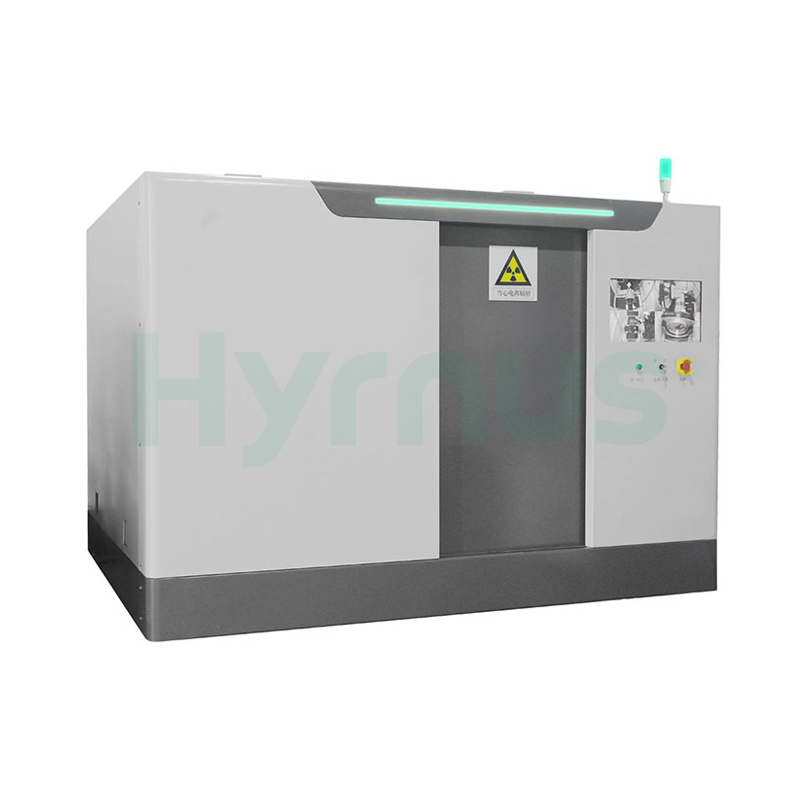
HY-XRB8101 fast 3D CT X-Ray system adopts X-ray penetration to complete non-destructive Open Hole (OH) flaw inspection for laminated power cell corners. Multi-angle scanning generates complete 3D volumetric data, and built-in AI algorithms realize automatic defect judgment to stabilize quality control during mass new energy cell manufacturing.
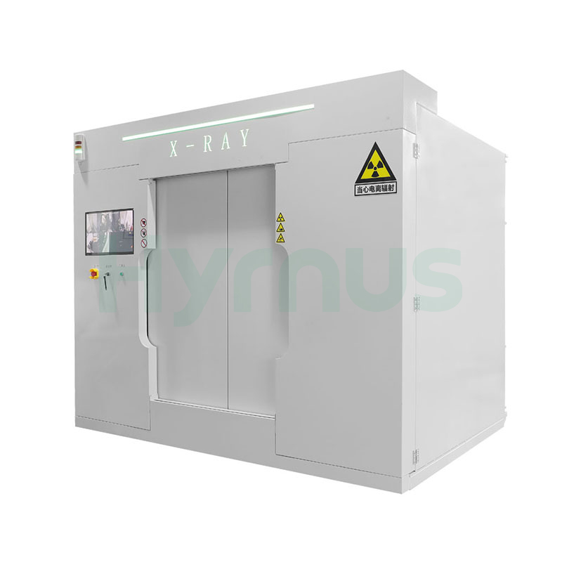
HY-XR8001 supports offline scanning and imaging for product Regions of Interest (ROI). Following 3D reconstruction, our dedicated visualization analysis software delivers accurate analytical measurement. Ideal for in-process quality control, failure analysis and laboratory research, the system performs fully non-destructive testing to visualize internal product structures and hidden defects, with complete measurement and analytical capabilities.
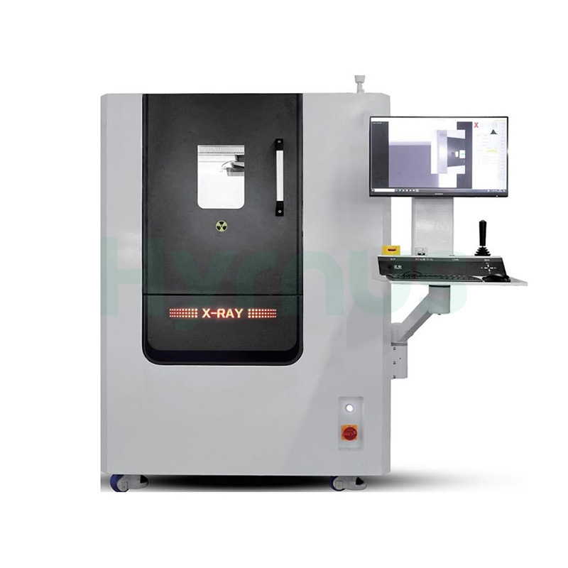
HY-XR5010A (2D) Series detects invisible internal flaws of industrial workpieces. It integrates micro-focus ray source, high-definition flat-panel imaging and CNC automatic inspection functions, equipped with reliable radiation protection design, suitable for offline quality control of medium-volume production lines across multiple manufacturing sectors.
leave a message
Scan To Wechat :

Scan To WhatsApp :