What Are You Looking For?


HY-WT9230 is developed for ultra-hard brittle semiconductor materials up to 12 inches. Built with dual air-bearing spindles and a high-precision grinding Z-axis, it supports fully automatic mirror thinning with high efficiency and damage-free processing. Equipped with a porous vacuum chuck and ultra-fine feed control, the machine ensures superior flatness and thickness uniformity for semiconductor wafer thinning processes.
Brand :
HYRNUSItem No. :
HY-WT9230Order(MOQ) :
1 SetWarranty :
One-Year Warranty and Lifetime MaintenancePayment :
T/TLead Time :
7-35 DaysProduct Origin :
ChinaWafer Thinning Machine for Hard and Brittle Semiconductor Materials

Product Introduction
HY-WT9230 Wafer Thinning Machine is suitable for various ultra-hard brittle semiconductor materials with diameters up to 12 inches. Equipped with dual air-bearing spindles and a high-precision grinding Z-axis, it performs fully automatic mirror thinning featuring high efficiency, zero workpiece damage and excellent thickness uniformity.
The machine adopts a porous ceramic vacuum chuck to hold wafers stably. It achieves a minimum feed of 0.1 μm, post-grinding TTV less than 3.0 μm, and surface roughness Ra<10 nm after fine grinding with an 8000# grinding wheel.
Machine Structure Diagram
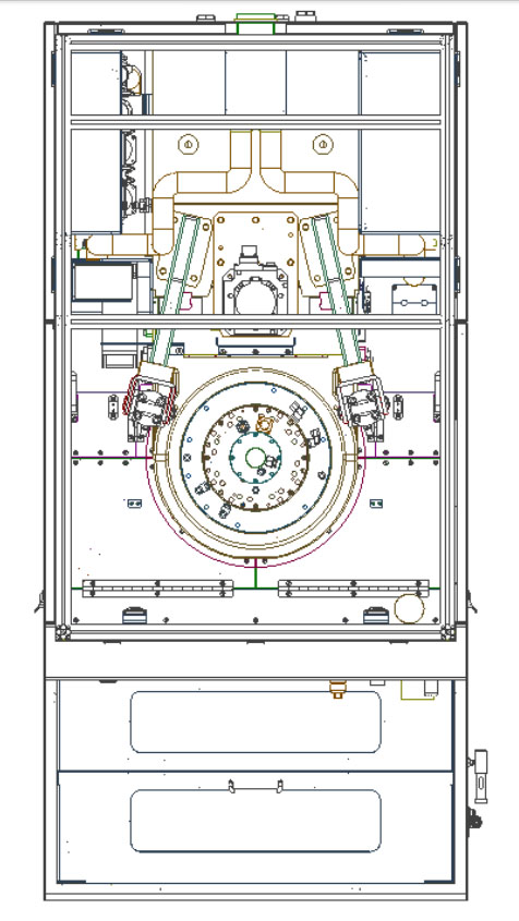
Machine Operation Process
| Step | Operation Steps |
| 1 | Manually place the wafer onto the ceramic chuck for automatic adsorption. |
| 2 | The transfer mechanism drives the workpiece spindle to the grinding station. |
| 3 | The grinding assembly automatically grinds the wafer down to the required thickness. |
| 4 | The transfer mechanism transports the ground wafer to the loading & unloading station. |
| 5 | Manually take out the processed wafer. |
Specifications
| Item | Parameters |
| Workpiece Size Range | Maximum processable size: Ø300mm |
| Grinding Wheel Air-bearing Spindle | Quantity: 1 |
| Spindle Power: 11.0KW | |
| Spindle Speed: 1000~4000r/min | |
| Workpiece Air-bearing Spindle | Quantity: 1 |
| Spindle Speed: 10~300r/min | |
| Grinding Z-axis | Travel: 120mm |
| Grinding Feed Speed: 0.0001~0.08mm/s | |
| Minimum Feed Increment: 0.1μm | |
| Clamping Method | Porous Vacuum Chuck |
| Post-grinding TTV | <3.0μm |
| Wafer-to-Wafer Thickness Deviation after Grinding | ±3μm |
| Surface Roughness after Fine Grinding | Ra<10nm (8000# grinding wheel) |
Main Frame
| No. | Item | Specification |
| 1 | Frame | Lower frame: Cast iron (standard configuration) |
| Upper frame: 30×60 aluminum profile | ||
| 2 | Cover Plate | Cold rolled steel plate with RAL9003 plastic spraying on surface (standard configuration) |
| 3 | Structural Parts | 45# steel with chrome-plated surface, anodized aluminum alloy and stainless steel |
| 4 | Power Supply | Three-phase 380 V, 50 Hz |
| 5 | Air Source | ≥0.5 MPa (fluctuation <0.03 MPa), 150 L/min |
| 6 | Water Source | Pressure: 0.2–0.3 MPa |
| Flow rate: >20 L/min | ||
| Temperature: Ambient temperature +2℃ (fluctuation ±1℃) | ||
| 7 | Power Consumption | Warm-up: 4 kW; Grinding: 8 kW |
Product Details
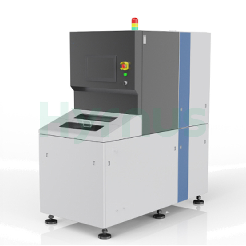
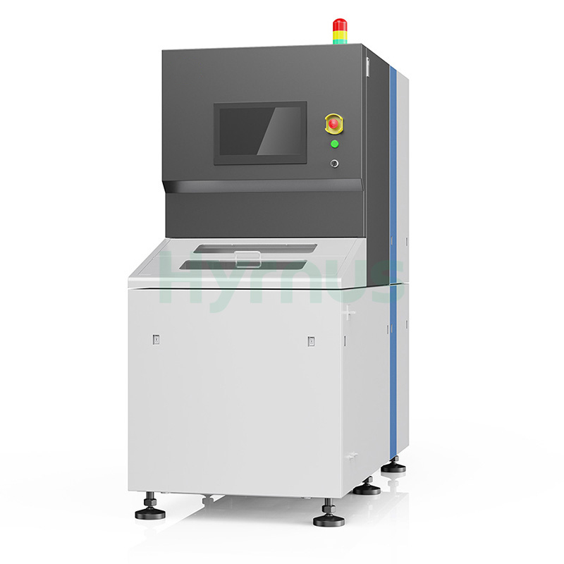
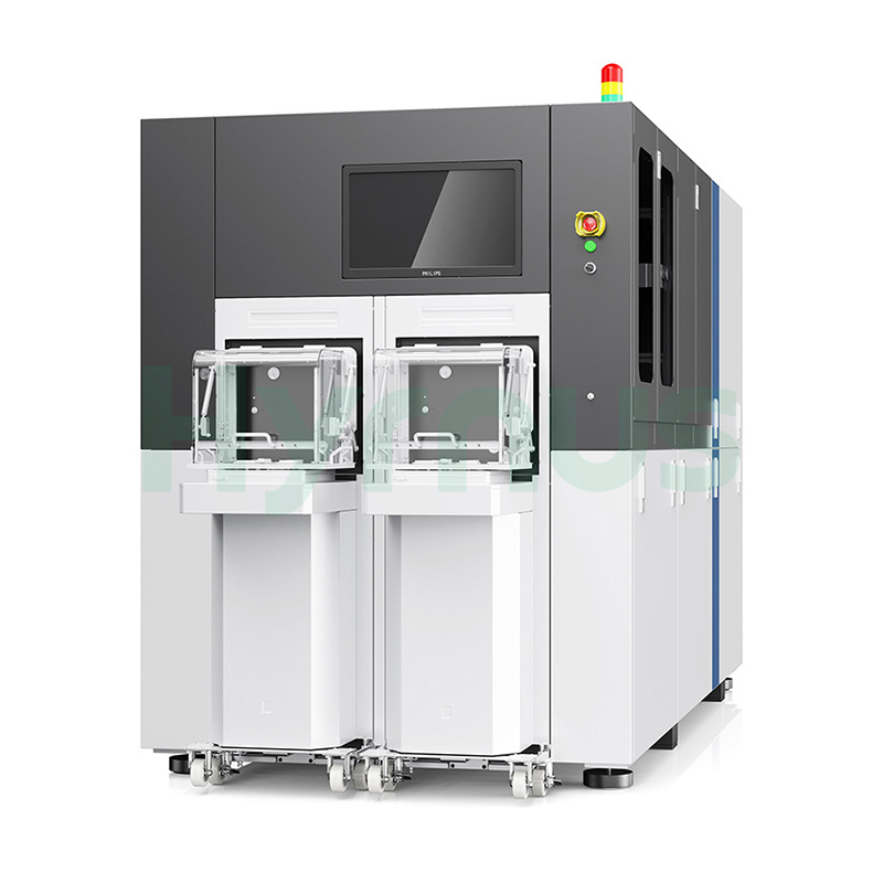
HY-WT9330 is equipped with one air-bearing grinding spindle and two air-bearing workpiece spindles. It can process various ultra-hard, brittle and hard-to-grind substrates up to 12 inches, enabling high-efficiency, damage-free and ultra-precise mirror grinding with outstanding thickness accuracy, suitable for the back thinning process of all types of chip wafers.
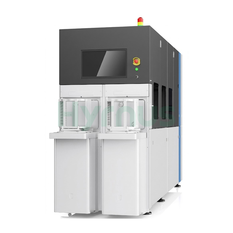
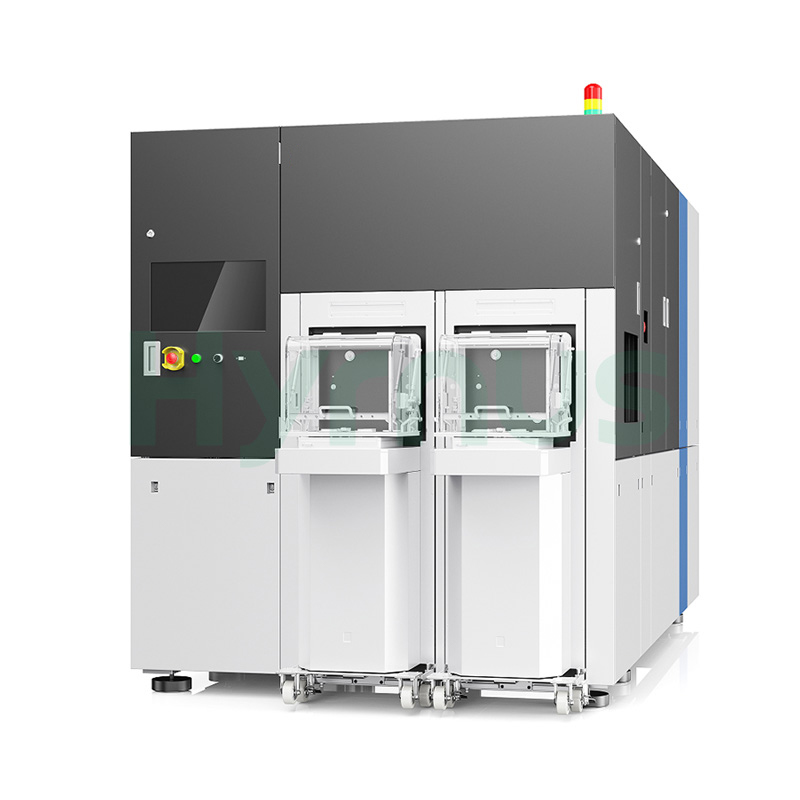
HY-WT9530 is fitted with 2 air-bearing spindles and 3 vacuum chuck tables for hard brittle substrates up to 8-inch. Operators only need to load cassettes manually, while the machine completes full automatic cycles including rough/fine grinding, cleaning and recovery. Post-grinding TTV≤1.5μm with excellent flatness and surface roughness, suitable for backside thinning of various semiconductor wafers.
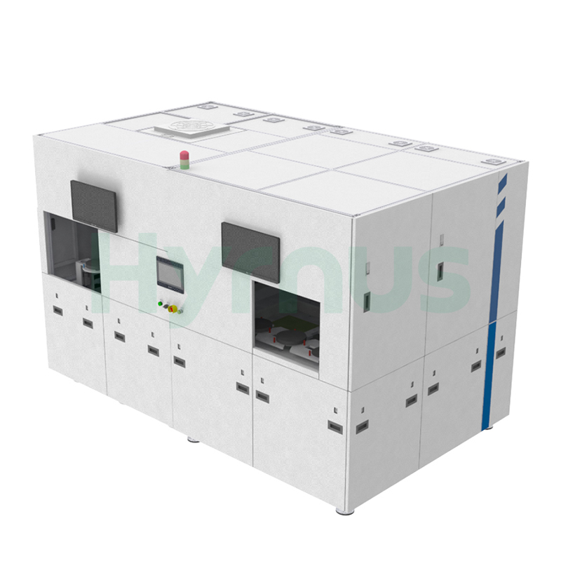
HY-WT9730 supports wafers up to 12-inch. Equipped with 3 grinding air-bearing spindles and 4 workpiece air-bearing spindles, it integrates rough grinding, fine grinding and polishing processes. The full robotic workflow automatically completes wafer transfer, processing, cleaning and unloading; only manual cassette feeding is needed. Ultra-precise Z-axis feed delivers superior wafer flatness and damage-free mirror polishing, while its sturdy frame guarantees stable mass production.
HY-IS1000 is dual-station SiC ingot laser slicing and grinding equipment combining laser modification and wafer delamination processes. It uses ultra-short pulse laser to form internal modified layers inside SiC ingots for saw-mark-free wafer splitting, delivering high throughput with ground wafer TTV ≤1.1 μm. It is essential mass-production equipment for third-generation semiconductor substrate manufacturing.
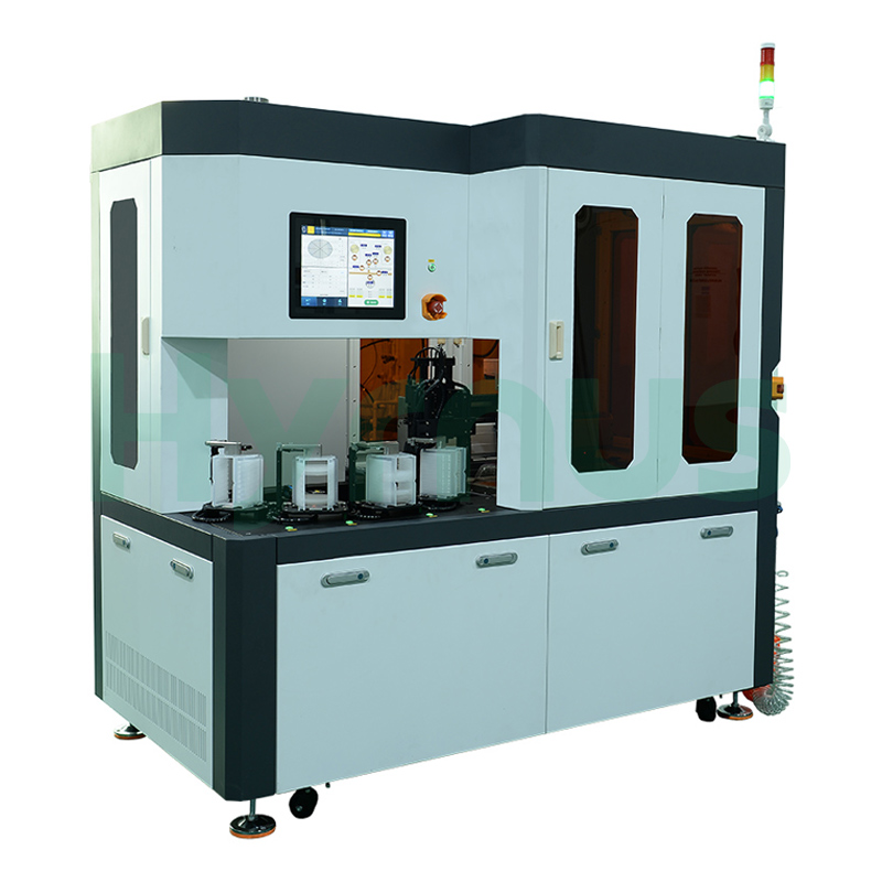
HY-WC615 double-side wafer chamfering machine is equipped with CCD vision positioning & online thickness measurement modules, self-developed core mechanical components and full auto loading/unloading system, delivering outstanding machining precision and user-friendly touch operation for wafer chamfer processing.
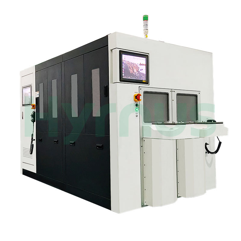
The HY-ST3005 handles 4–12 inch hard brittle semiconductor substrates for high-precision back thinning. Iteratively upgraded for superior accuracy and long-term stability, it features premium core assemblies (hydrostatic air-bearing grinding spindle, high-precision wafer spindle, high-rigidity large-diameter rotary table) and high automation for mass production of silicon and compound semiconductor wafers.
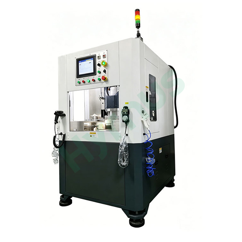
The HY-ST3002 handles 4–12 inch wafers for precision thinning and grinding of hard brittle semiconductors. Fully upgraded with mature processes, it features enhanced accuracy and stable long-run performance, with refined automatic thinning architecture and premium key parts: hydrostatic air-bearing grinding spindle, hydrostatic air-bearing wafer holding spindle, high-rigidity large-diameter rotary table.
leave a message
Scan To Wechat :

Scan To WhatsApp :