What Are You Looking For?


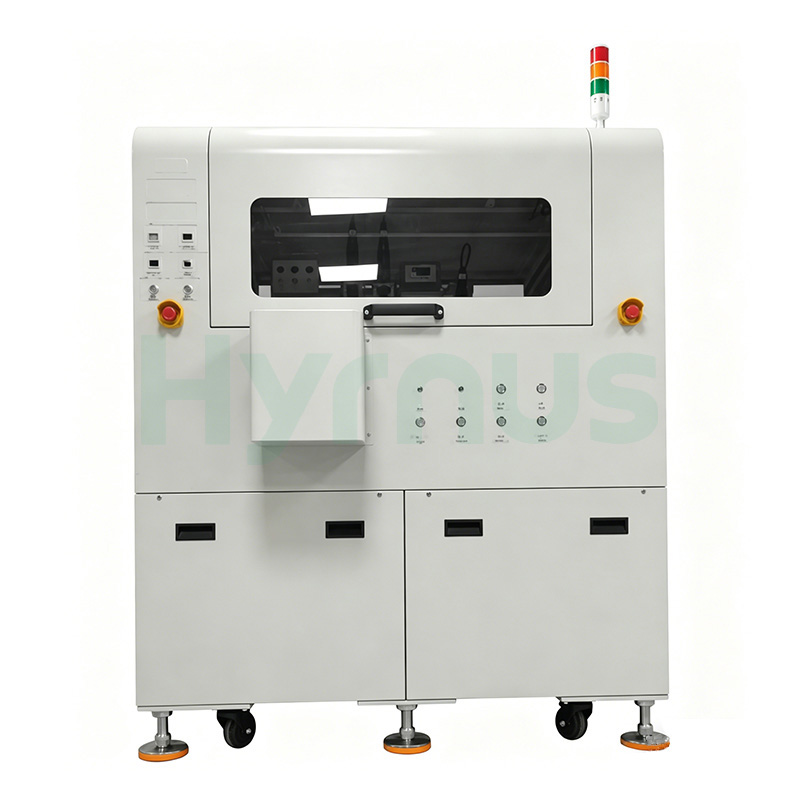
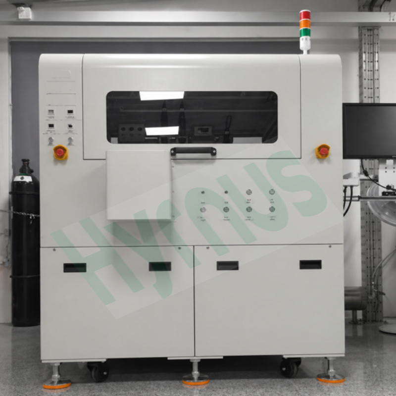
HY-DB504 Die Bonder is a Fully Automatic Die Bonder developed for Ultra-High-Precision Optoelectronic and Semiconductor Packaging applications.
Brand :
HYRNUSItem No. :
HY-DB504Order(MOQ) :
1 SetWarranty :
One-Year Warranty and Lifetime MaintenancePayment :
T/TLead Time :
7-35 DaysProduct Origin :
ChinaDie Bonder for Ultra-High-Precision Optoelectronic and Semiconductor Packaging applications

Product Introduction
HY-DB504 Die attach equipment With extreme placement accuracy as its core advantage, the equipment is widely used in TO-Series Devices, Photodiodes, Lasers, Optocouplers, miniLEDs, and Consumer Optoelectronic Devices, making it particularly suitable for cutting-edge product development and high-volume production that demands the highest levels of placement precision.
Application Scenarios
TO series devices, photodiodes, lasers, optocouplers, miniLEDs, consumer electronics optoelectronic devices, etc.
Product Feature
High-precision automatic chip angle correction system
Automatic PCB change (single or dual magazine configuration available)
Constant-temperature dispensing function
Missing die detection
Nozzle clogging detection
Dual in-line bond head for high die bonding accuracy
Pre-dispensing inspection
Technical Specifications
| No | Category | Parameter | Specification |
| 1. General Information | Operating System | Windows 7 | |
| Supported Languages | Chinese / English | ||
| UPH | 1K/H (Max) (varies depending on material and quality requirements) | ||
| 2. Precision | X/Y Die Bonding Accuracy | ±3 μm (excluding photomask and raw material errors) | |
| Angle Accuracy | ±0.5° | ||
| 3. Automation | Automatic PCB Change | Yes | |
| Automatic Wafer Ring Change | Optional | ||
| 4. Vision System | Camera Resolution | 1280 × 1024 pixels | |
| Inspection Functions | High-intelligence vision system, supports automatic inspection of glue volume, shape, position, and post-bond inspection | ||
| 5. Compatibility | System Compatibility | Supports multiple map formats | |
| Customization | High openness, customizable according to different customer requirements | ||
| 6. Dimensions & Weight | PCB Size (W×L, max) | 90 mm × 280 mm | |
| Die Size | 6 mil × 6 mil ~ 100 mil × 100 mil | ||
| Wafer Ring Size | 6 inch (other sizes customizable) | ||
| Equipment Dimensions (L×W×H) | 1600 × 1000 × 1630 mm | ||
| Equipment Weight | 1050 kg (final weight subject to actual product) | ||
| 7. Utilities | Compressed Air | 5–6 kgf/cm² | |
Product Details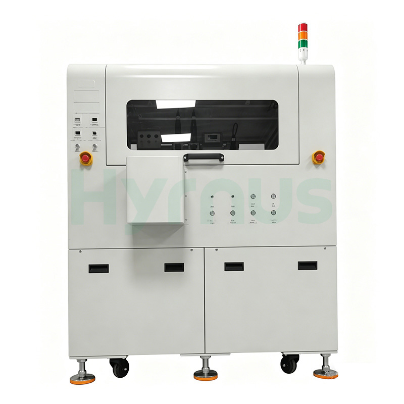
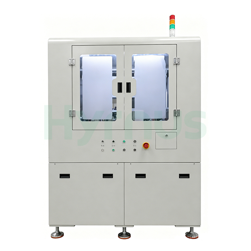
HY-ED022 Die Bonder is developed for Optical Communication and Optical Device Packaging applications.
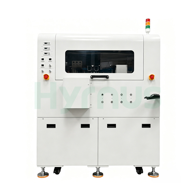
HY-ED010 Die Bonding Machine is a Die bonding machine developed for Automotive LED and Optoelectronic Semiconductor Packaging applications.
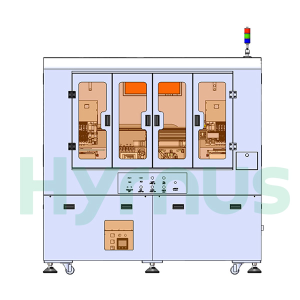
HY-ED007 Die Attach Machine is a High-Precision Die attach machine developed for Optical Communication, Optical Modules, Multi-Chip Modules (MCM), 3D Packaging, and Optoelectronic Device applications.
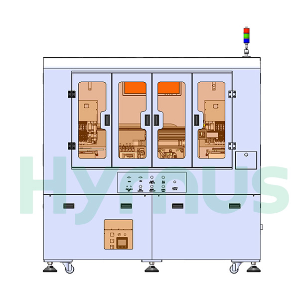
HY-ED003 Die Attach Equipment is a High-Precision Eutectic Bonder developed for Optical Communication, Optical Modules, Multi-Chip Modules (MCM), 3D Packaging, and Optoelectronic Device applications.
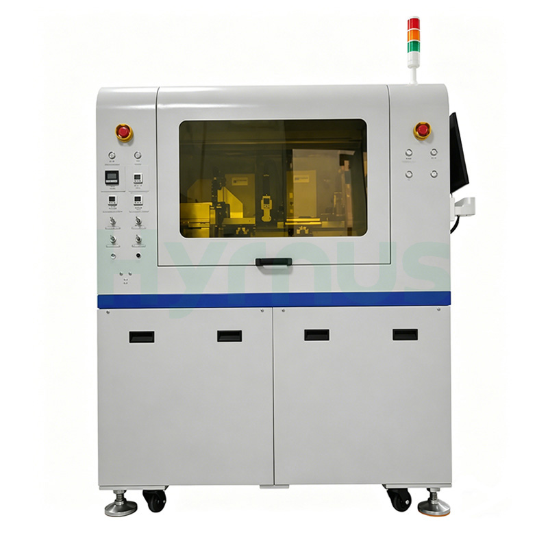
HY-DB503 Die Bonder is a High-Speed Fully Automatic Die Bonder developed for Optoelectronic and Semiconductor Packaging applications.
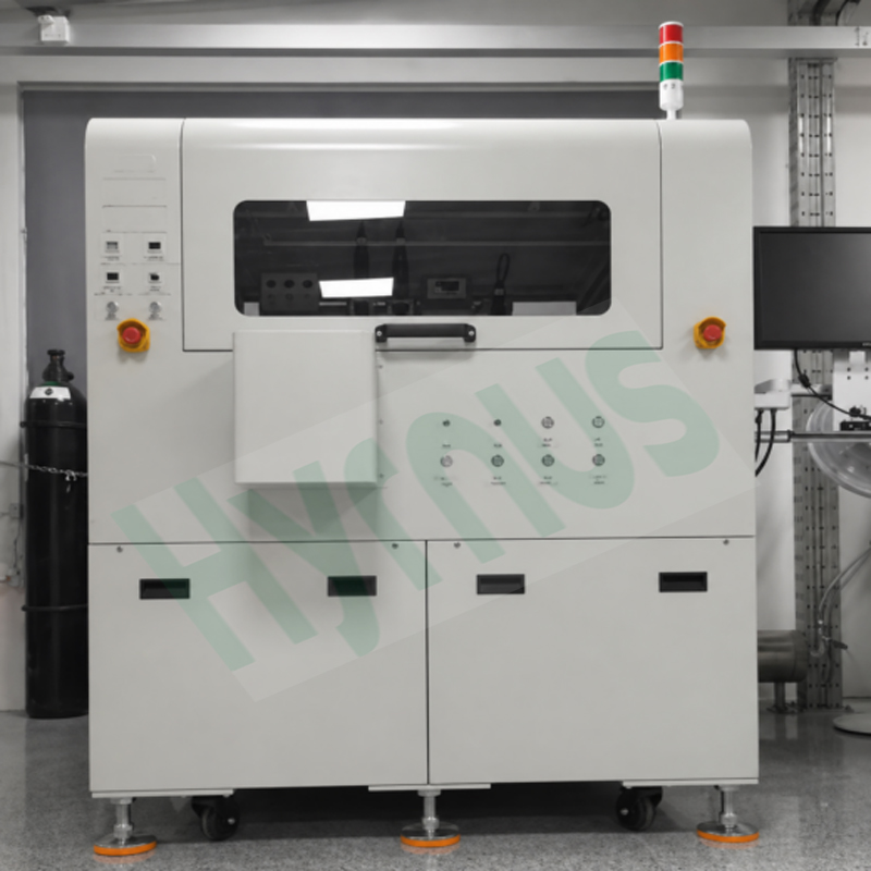
HY-DB501 Die Bonder is a fully automatic die bonder developed for ultra-high-precision optoelectronic and semiconductor packaging applications.It delivers precision-driven die attachment for optoelectronic packaging, targeting TO‑series devices, photodiodes, lasers, optocouplers, and miniLEDs with placement accuracy of ±5 μm and angular control within ±1°.
HY-DB500 Die Bonder is a high-end, fully automatic die bonder engineered for optoelectronic devices and high-precision semiconductor packaging. Built with exceptional stability, intelligent control, and a modular architecture, it is ideally suited for high-volume production of TO-series devices, photodiodes, lasers, optocouplers, miniLEDs, and consumer optoelectronic components.
leave a message
Scan To Wechat :

Scan To WhatsApp :