What Are You Looking For?


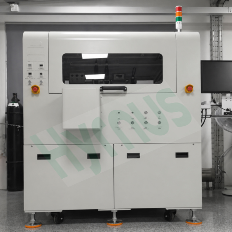
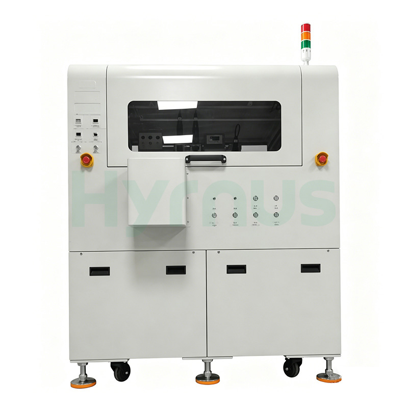
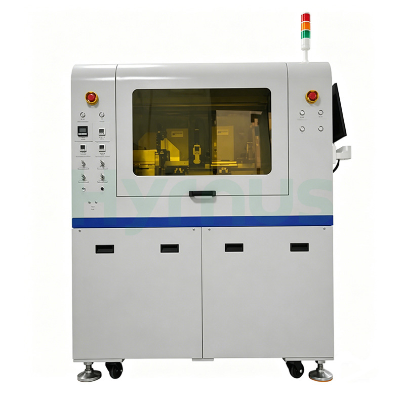
HY-DB501 Die Bonder is a fully automatic die bonder developed for ultra-high-precision optoelectronic and semiconductor packaging applications.It delivers precision-driven die attachment for optoelectronic packaging, targeting TO‑series devices, photodiodes, lasers, optocouplers, and miniLEDs with placement accuracy of ±5 μm and angular control within ±1°.
Brand :
HYRNUSItem No. :
HY-DB501Order(MOQ) :
1 SetWarranty :
One-Year Warranty and Lifetime MaintenancePayment :
T/TLead Time :
7-35 DaysProduct Origin :
ChinaFully Automatic Die Bonder for Ultra-High-Precision Optoelectronic

Product Introduction
HY-DB501 Die Bonding machine with extreme accuracy as its core advantage, the equipment is widely used in TO-series devices, photodiodes, lasers, optocouplers, miniLEDs, and consumer optoelectronic devices, making it particularly suitable for high-volume production of high-end products that demand stringent placement accuracy.Dual in‑line bond head architecture maintains stability across continuous operation, while the intelligent vision engine conducts three inspection checkpoints—pre‑dispensing surface verification, glue quantity and profile validation, and post‑bond alignment auditing—to intercept defects before they compromise assembly integrity. Automatic PCB exchange supports both single and dual magazine layouts, sustaining material flow without operator reloading. The system accommodates 6‑inch wafer rings and PCBs sized 90×280 mm, with optional UV curing and automatic wafer ring change expanding process coverage. Innovative power‑off collision prevention operates independently of UPS, lowering auxiliary equipment costs while protecting tooling during outages. Built on Windows 7 with bilingual interface support, the HY-DB501 offers parametric configurability for diverse die sizes from 6×6 mil to 100×100 mil.
Application Scenarios
TO series devices, photodiodes, lasers, optocouplers, miniLEDs, consumer electronics optoelectronic devices, etc
Product Feature
This high-precision automatic die bonding system features automatic chip angle correction, automatic PCB change (single or dual magazine), and constant-temperature dispensing. Quality assurance is ensured through missing die detection, nozzle clogging detection, pre-dispensing inspection, glue amount detection, and post-bond inspection, with a dual in-line bond head delivering high bonding accuracy. It supports 6-inch and smaller wafer rings (other sizes customizable), optional UV PCB curing, and power-off anti-collision protection without UPS. Multiple configurations and full customization are available.
Technical Specifications
| No | Category | Parameter | Specification |
| 1. General Information | Equipment Name | HY-DB501 | |
| Operating System | Windows 7 | ||
| Supported Languages | Chinese / English | ||
| UPH | 2K/H (Max) (varies depending on material and quality requirements) | ||
| 2. Precision | X/Y Die Bonding Accuracy | ±5 μm (excluding photomask and raw material errors) | |
| Angle Accuracy | ±1° | ||
| 3. Vision System | Camera Resolution | 1280 × 1024 pixels | |
| Inspection Functions | High-intelligence vision system, supports automatic inspection of glue volume, shape, position, and post-bond inspection | ||
| 4. Automation | Automatic PCB Change | Yes | |
| Automatic Wafer Ring Change | Optional | ||
| 5. Compatibility | System Compatibility | Supports multiple map formats | |
| Customization | High openness, customizable according to different customer requirements | ||
| 6. Dimensions & Weight | PCB Size (W×L, max) | 90 mm × 280 mm | |
| Die Size | 6 mil × 6 mil ~ 100 mil × 100 mil | ||
| Wafer Ring Size | 6 inch (other sizes customizable) | ||
| Equipment Dimensions (L×W×H) | 1600 × 1000 × 1630 mm | ||
| Equipment Weight | 1050 kg (final weight subject to actual product) | ||
| 7. Utilities | Compressed Air | 5–6 kgf/cm² | |
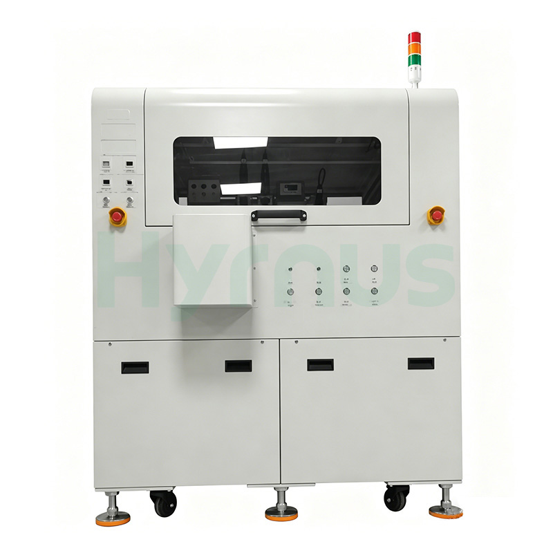
Product Details
 FAQs
FAQs
The HY-DB501 achieves a maximum UPH of 2,000 units per hour. Please note that actual throughput may vary depending on material characteristics and specific quality requirements.
The system delivers X/Y die bonding accuracy of ±5 μm (excluding photomask and raw material errors) and angle accuracy of ±1°, ensuring high-precision placement for optoelectronic and semiconductor devices.
The high-intelligence vision system supports pre-dispensing inspection, glue amount and shape detection, glue position verification, and post-bond inspection, providing comprehensive quality assurance throughout the bonding process.
the system offers high openness with multiple configurations available. It supports 6-inch wafer rings (other sizes customizable), automatic PCB change with single or dual magazine options, automatic wafer ring change (optional), and UV PCB curing function (optional). Customization is available to meet specific customer needs.
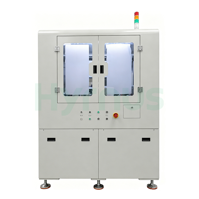
HY-ED022 Die Bonder is developed for Optical Communication and Optical Device Packaging applications.
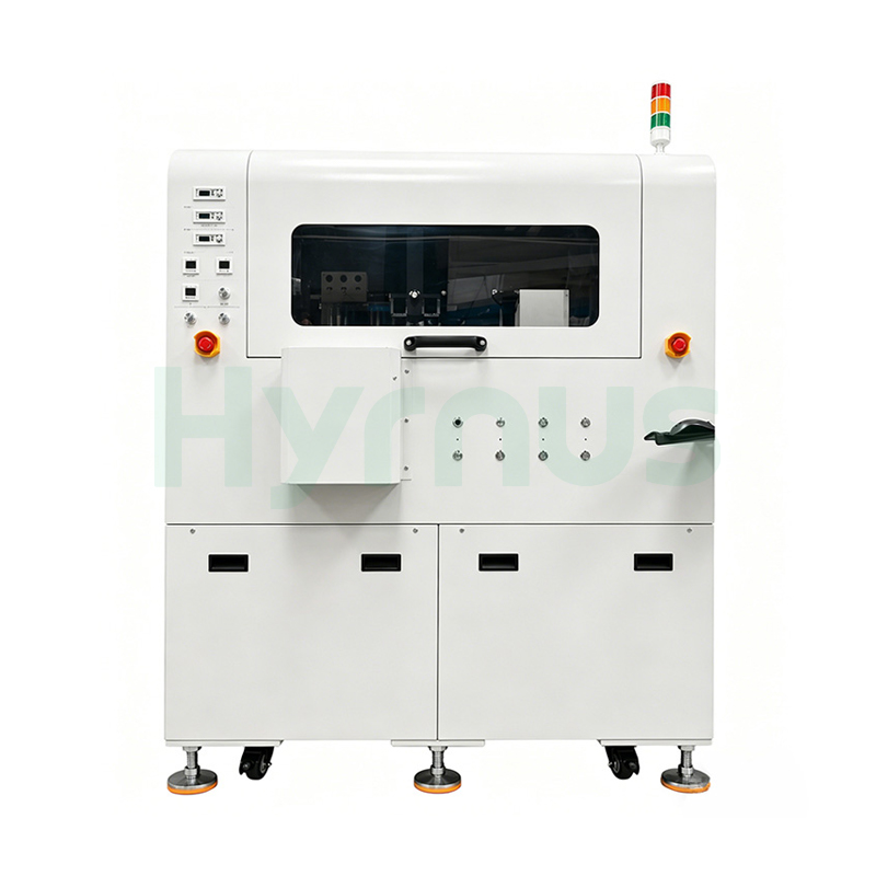
HY-ED010 Die Bonding Machine is a Die bonding machine developed for Automotive LED and Optoelectronic Semiconductor Packaging applications.
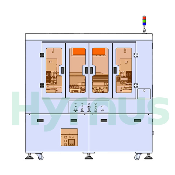
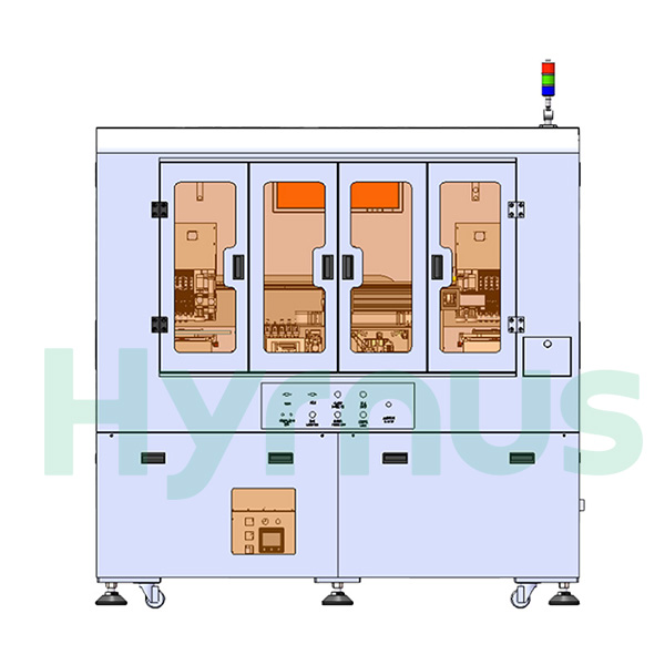
HY-ED007 Die Attach Machine is a High-Precision Die attach machine developed for Optical Communication, Optical Modules, Multi-Chip Modules (MCM), 3D Packaging, and Optoelectronic Device applications.
HY-ED003 Die Attach Equipment is a High-Precision Eutectic Bonder developed for Optical Communication, Optical Modules, Multi-Chip Modules (MCM), 3D Packaging, and Optoelectronic Device applications.
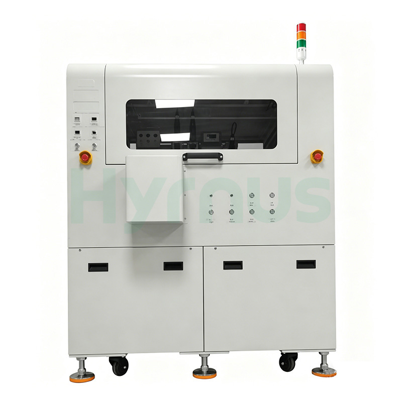
HY-DB504 Die Bonder is a Fully Automatic Die Bonder developed for Ultra-High-Precision Optoelectronic and Semiconductor Packaging applications.
HY-DB503 Die Bonder is a High-Speed Fully Automatic Die Bonder developed for Optoelectronic and Semiconductor Packaging applications.
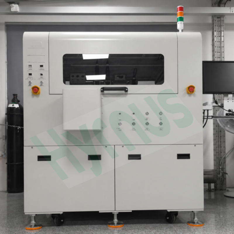
HY-DB500 Die Bonder is a high-end, fully automatic die bonder engineered for optoelectronic devices and high-precision semiconductor packaging. Built with exceptional stability, intelligent control, and a modular architecture, it is ideally suited for high-volume production of TO-series devices, photodiodes, lasers, optocouplers, miniLEDs, and consumer optoelectronic components.
leave a message
Scan To Wechat :

Scan To WhatsApp :