What Are You Looking For?


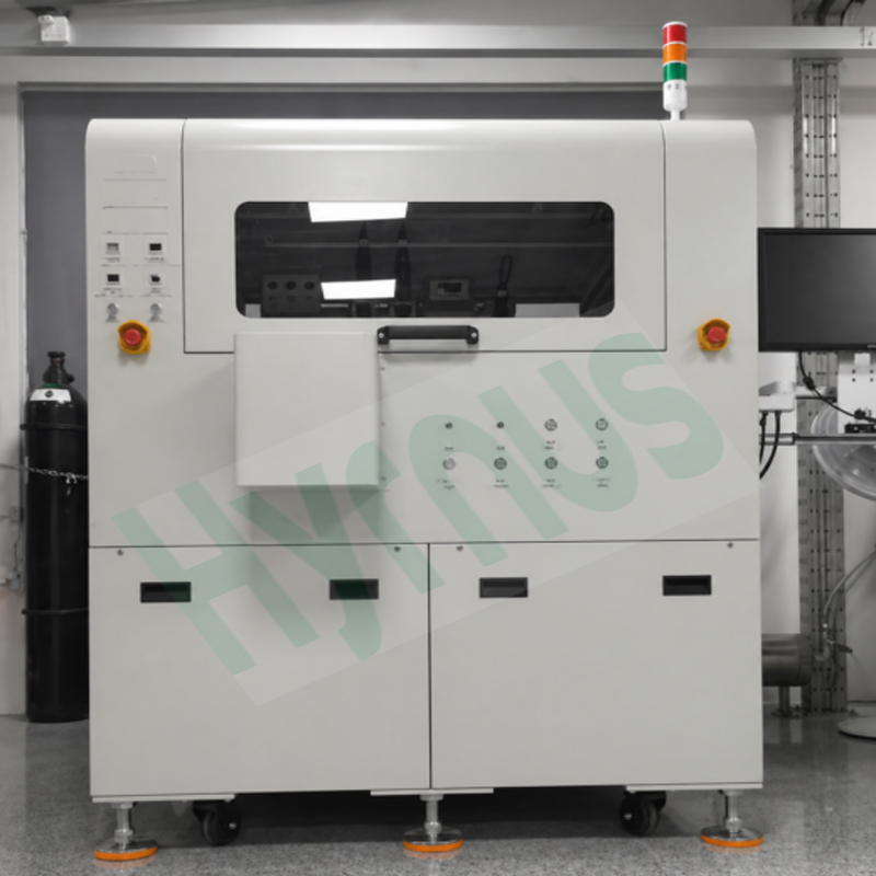
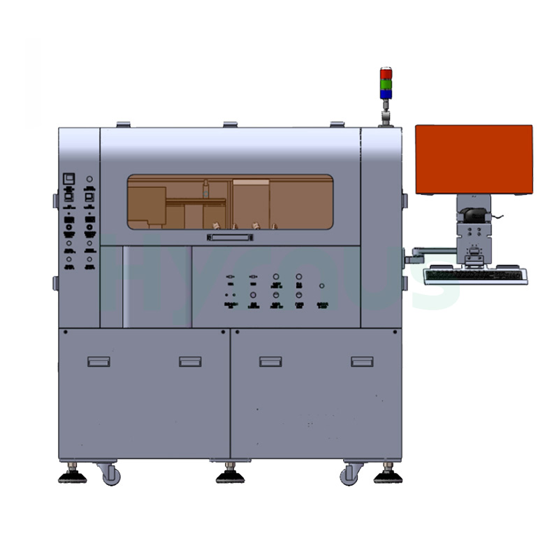
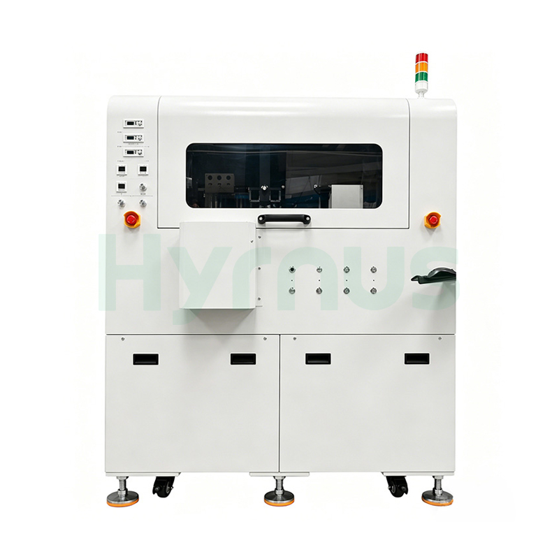
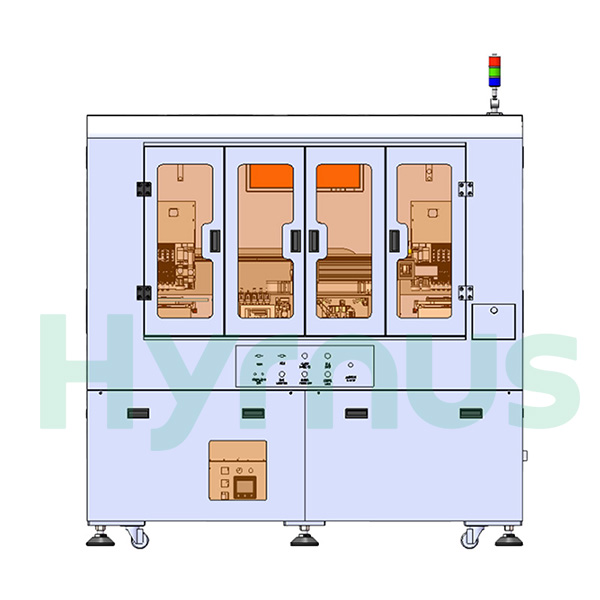
HY-DB500 Die Bonder is a high-end, fully automatic die bonder engineered for optoelectronic devices and high-precision semiconductor packaging. Built with exceptional stability, intelligent control, and a modular architecture, it is ideally suited for high-volume production of TO-series devices, photodiodes, lasers, optocouplers, miniLEDs, and consumer optoelectronic components.
Brand :
HYRNUSItem No. :
HY-DB500Order(MOQ) :
1 SetWarranty :
One-Year Warranty and Lifetime MaintenancePayment :
T/TLead Time :
7-35 DaysProduct Origin :
ChinaFully Automatic Die Bonder for Semiconductor Packaging

Product Introduction
HY-DB500 Die Attach Machine achieves a throughput of 6,000 units per hour with ±10 μm XY placement accuracy (achievable ±8 μm) and ±1° angular precision, ensuring consistent, reliable die attachment for demanding optical and electronic applications. The linear high-precision bond head delivers exceptional stability during high-speed operation, while the high-intelligence vision system performs comprehensive pre-dispensing inspection, glue volume and shape verification, and post-bond placement validation—catching defects early and protecting downstream yield. The system features automatic PCB changeover with magazine configuration options, automatic wafer ring change, and automatic loading/unloading functionality, significantly reducing operator intervention for sustained continuous production. Compatible with 6-inch wafer rings and PCBs up to 280×90 mm, with die sizes ranging from 6×6 mil to 100×100 mil, the HY-DB500 offers remarkable flexibility for high-mix assembly lines. Innovative power-off anti-collision protection eliminates the need for UPS, reducing infrastructure costs while safeguarding tooling and workpieces during unexpected shutdowns. Additional UV curing capability and customizable configurations further extend application coverage. With Windows 7-based operation, bilingual interface, and high openness for customization, the HY-DB500 adapts to evolving production demands—delivering the precision, productivity, and investment protection that optoelectronic packaging professionals require.
Product Features
Technical Specifications
| No | Category | Parameter | Specification |
| 1. General Information | Equipment Name | HY-DB500 | |
| Operating System | Windows 7 | ||
| Supported Languages | Chinese / English | ||
| UPH | 6K/H (varies depending on material and quality requirements) | ||
| 2. Precision | XY Die Bonding Accuracy | ±10 μm (achievable ±8 μm) | |
| Angle Accuracy | ±1° | ||
| Bond Head Type | Linear high-precision die bonding head | ||
| 3. Vision System | Camera Resolution | 1280 × 1024 pixels | |
| Inspection Functions | Supports automatic inspection of glue volume, shape, position, and post-bond inspection | ||
| 4. Automation (Optional) | Automatic PCB Change | Yes | |
| Automatic Wafer Ring Change | Yes | ||
| 5. Compatibility | Compatibility | Supports multiple map formats | |
| Customization | High openness, customizable according to customer requirements | ||
| 6. Dimensions & Weight | PCB Size (L×W, max) | 280 mm × 90 mm (other sizes customizable) | |
| Wafer Ring Size | 6 inch (other sizes customizable) | ||
| Die Size | 6 mil × 6 mil ~ 100 mil × 100 mil | ||
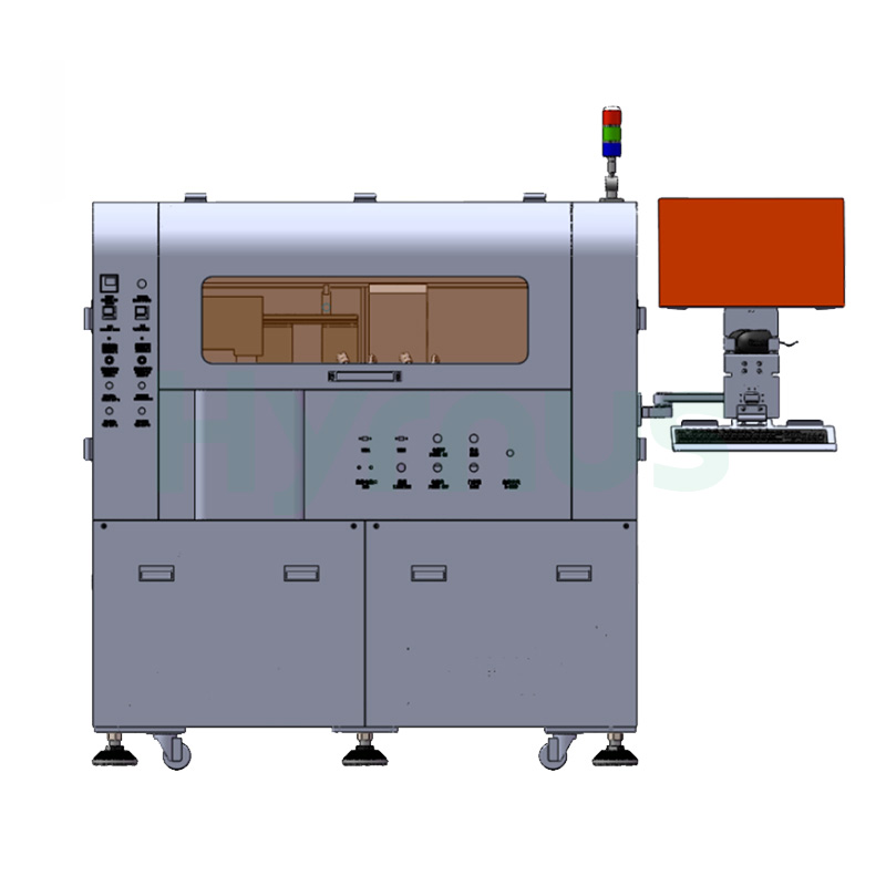
| Equipment Dimensions (L×W×H) | 1600 × 1000 × 1630 mm | ||
| Equipment Weight | 1050 kg (final weight subject to actual product) | ||
| 7. Utilities | Compressed Air | 5–6 kgf/cm² | |
Product Details
 FAQs
FAQs
The HY-DB500 delivers a maximum throughput of 6,000 units per hour, with XY placement accuracy of ±10 μm (achievable ±8 μm) and angular precision of ±1°. This combination of speed and precision makes the system ideal for high-volume optoelectronic assembly where both productivity and placement integrity are critical.
The system supports a wide range of optoelectronic devices including TO-series components, photodiodes, lasers, optocouplers, and miniLEDs, as well as general consumer optoelectronics. It accommodates die sizes from 6×6 mil to 100×100 mil, 6-inch wafer rings, and PCBs up to 280×90 mm. Other wafer ring sizes and PCB dimensions can be customized to meet specific production requirements.
The high-intelligence vision system performs three critical inspection functions: pre-dispensing inspection to detect debris or defects on the PCB before adhesive application, glue amount detection to verify volume and presence, and post-bond inspection to confirm die placement position and angle. This closed-loop quality assurance ensures that defects are identified immediately, preventing faulty assemblies from progressing downstream.
The HY-DB500 incorporates an innovative power-off anti-collision protection function that operates without requiring an uninterruptible power supply (UPS). During unexpected power outages, the system prevents collision between the bond head and workpieces, protecting valuable tooling and partially processed assemblies from damage. This reduces repair costs, minimizes restart delays, and eliminates the expense of UPS infrastructure—delivering both operational and financial advantages.
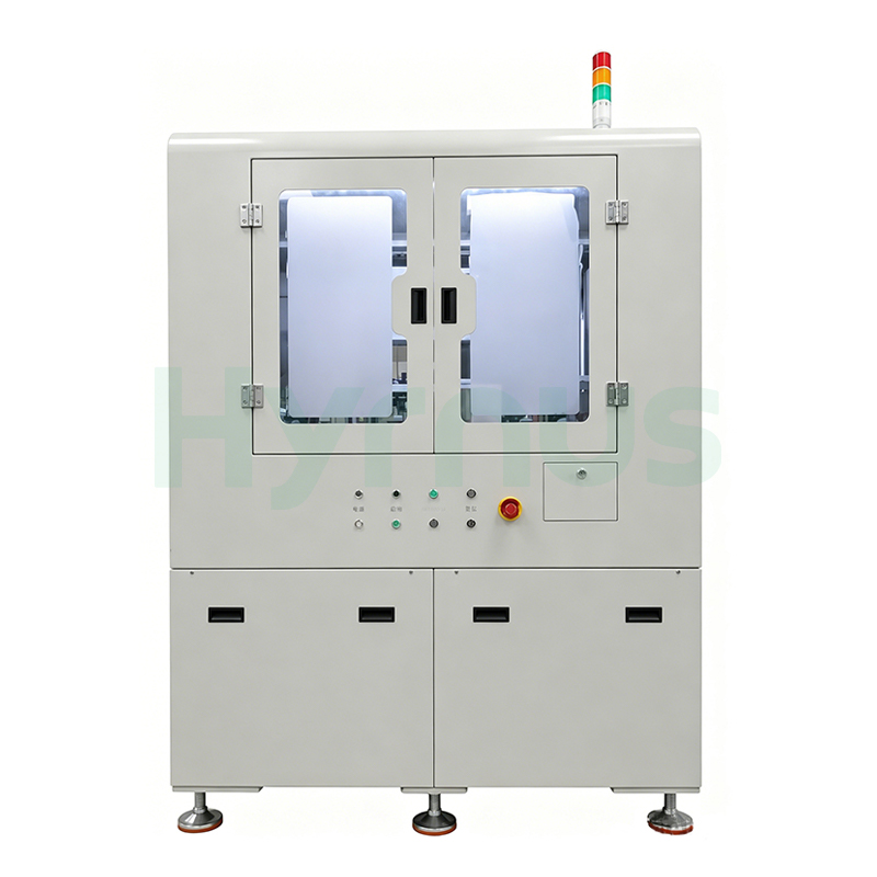
HY-ED022 Die Bonder is developed for Optical Communication and Optical Device Packaging applications.
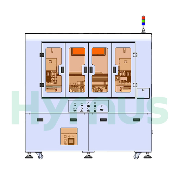
HY-ED010 Die Bonding Machine is a Die bonding machine developed for Automotive LED and Optoelectronic Semiconductor Packaging applications.
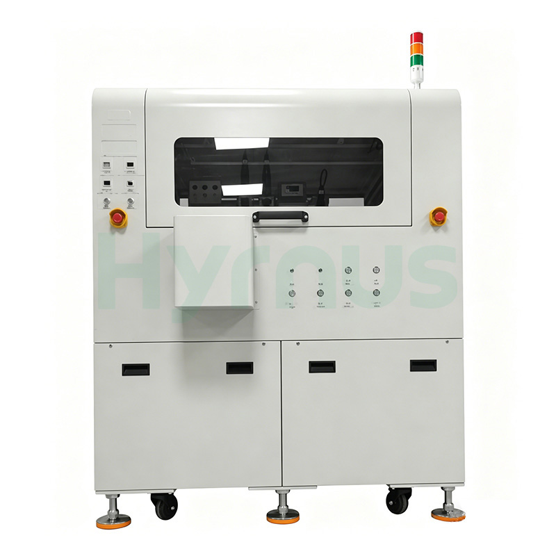
HY-ED007 Die Attach Machine is a High-Precision Die attach machine developed for Optical Communication, Optical Modules, Multi-Chip Modules (MCM), 3D Packaging, and Optoelectronic Device applications.
HY-ED003 Die Attach Equipment is a High-Precision Eutectic Bonder developed for Optical Communication, Optical Modules, Multi-Chip Modules (MCM), 3D Packaging, and Optoelectronic Device applications.
HY-DB504 Die Bonder is a Fully Automatic Die Bonder developed for Ultra-High-Precision Optoelectronic and Semiconductor Packaging applications.
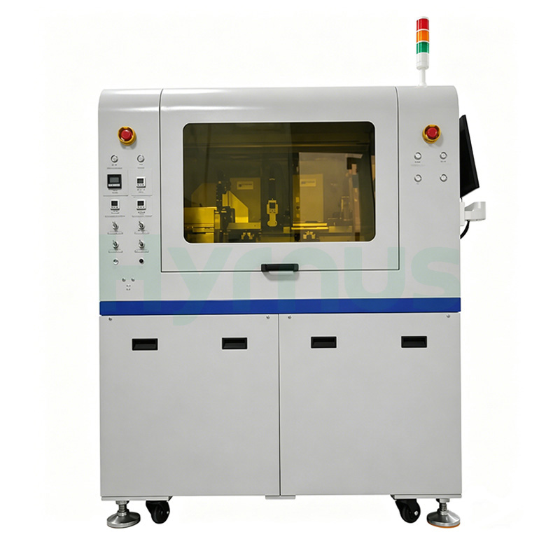
HY-DB503 Die Bonder is a High-Speed Fully Automatic Die Bonder developed for Optoelectronic and Semiconductor Packaging applications.
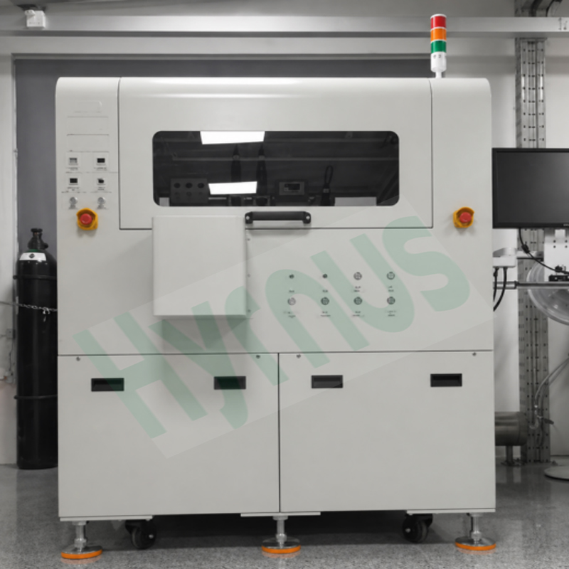
HY-DB501 Die Bonder is a fully automatic die bonder developed for ultra-high-precision optoelectronic and semiconductor packaging applications.It delivers precision-driven die attachment for optoelectronic packaging, targeting TO‑series devices, photodiodes, lasers, optocouplers, and miniLEDs with placement accuracy of ±5 μm and angular control within ±1°.
leave a message
Scan To Wechat :

Scan To WhatsApp :