What Are You Looking For?


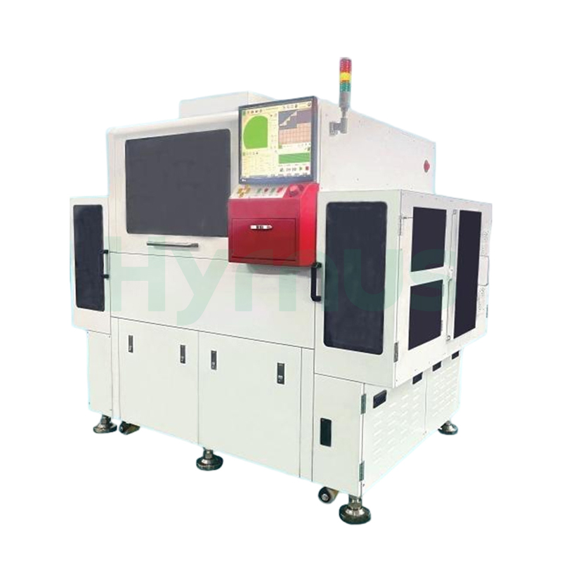
HY-DP200 Die Bonder is a high-speed, high-precision die bonding system engineered for ultra-thin and advanced semiconductor packaging applications, supporting IC, LSI, BGA, CSP, QFN, NAND Flash, Mobile DRAM, eMMC, SiP, and small-die devices.
Brand :
HYRNUSItem No. :
HY-DP200Order(MOQ) :
1 SetWarranty :
One-Year Warranty and Lifetime MaintenancePayment :
T/TLead Time :
7-35 DaysProduct Origin :
ChinaHigh-Speed & High-Precision Ultra-thin Die Bonder for advanced semiconductor packaging

Product Introduction
HY-DP200 Die bonding machine delivers a throughput of 6K UPH for epoxy bonding and 3.5K UPH for DAF bonding, with bond accuracy of ±10 µm (X/Y) and ±0.1° (θ), and epoxy bond accuracy of ±20 µm (X/Y) and ±1.0° (θ). The system accommodates die sizes from 0.5 mm to 20 mm, handles 8" and 12" wafers with auto-theta alignment and auto-expanding functions, and supports substrates up to 300 mm in length. Equipped with a 5-megapixel vision camera (2048 × 2048 pixels) and 256-level grayscale pattern recognition, it achieves position accuracy of ±4 pixels and angular accuracy of ±0.01° over a 20 × 20 mm FOV. The bond head provides bonding force from 0.5N to 30N (optional) with load cell auto-calibration, pre/post vision inspection, and Z-level auto-calibration. Operating on AC 200–240V ±10% single-phase 50/60Hz with a power consumption of approximately 2.2 kW, it requires compressed air over 5 kgf/cm² and vacuum below -750 mmHg. With dimensions of 2200 mm × 1460 mm × 1800 mm (with FFU) and a weight of approximately 2300 kg, the HY-DP200 offers high reliability with MTBA of 120 minutes and MTBF of 168 hours in a Class 1000 clean environment, making it an ideal solution for precision die attachment in high-volume manufacturing.
Key Technical Specifications
| HY-DP200 Series Specifications | ||
| System Productivity | UPH | |
| DAF: 3.5K UPH, Epoxy: 6K UPH | ||
| Application Package | IC, LSI, BGA, CSP, QFN, NAND Flash, Mobile DRAM, eMMC, SiP, Small Die | |
| System Capability | Epoxy Bond Accuracy | X/Y: ±20 µm, θ: ±1.0° |
| Bond Accuracy | X/Y: ±10 µm, θ: ±0.1° | |
| MTBA | 120 minutes | |
| MTBF | 168 hours | |
| Clean Class | 1000 Class | |
| Control | PC-based | |
| Bond Method | Epoxy Paste & DAF | |
| Material Handling Capability | Die Size | 0.5 - 20 mm |
| Substrate | Length: 100 - 300 mm; Width: 50 - 100 mm | |
| Magazine | Length: 110 - 320 mm; Width: 40 - 110 mm; Height: 100 - 190 mm | |
| Wafer System | Wafer Handling | 8", 12" |
| Auto-Theta Alignment | 360° Rotation | |
| Auto-Expanding | 10 mm | |
| Bond Head | Bond Force | 0.5 - 5N ±15%, 5 - 30N ±5% (Up to 30N: optional) |
| Bond Head Axis | X-Y-Z-Theta Axis (Single) | |
| Measure & Inspection System | Features | Force auto calibration of Load cell reedback,Pre/Post Vision Inspection Z level auto calibration |
| Pattern Recognition System | PR System | 256 Grey Levels |
| Camera | 5 mega vision camera (2048 × 2048) | |
| FOV | 20 × 20 mm | |
| Position Accuracy | ±4 pixel | |
| Angular Accuracy | ±0.01° | |
| Electrical Parameters | Voltage | AC 200~240V ±10% |
| Frequency | Single-phase 50/60Hz | |
| Compressed Air | Over 5 kgf/cm² | |
| Vacuum | -750 mmHg below | |
| Power Consumption | Approx. 2.2 kW | |
| Size/Weight (Estimate) | Dimensions (W × D × H) | 2200 × 1460 × 1800 mm (with FFU 115H) |
| Net Weight | Approx. 2300 kg | |
Product Details
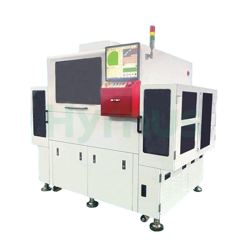
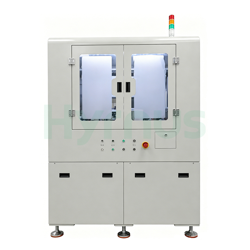
HY-ED022 Die Bonder is developed for Optical Communication and Optical Device Packaging applications.
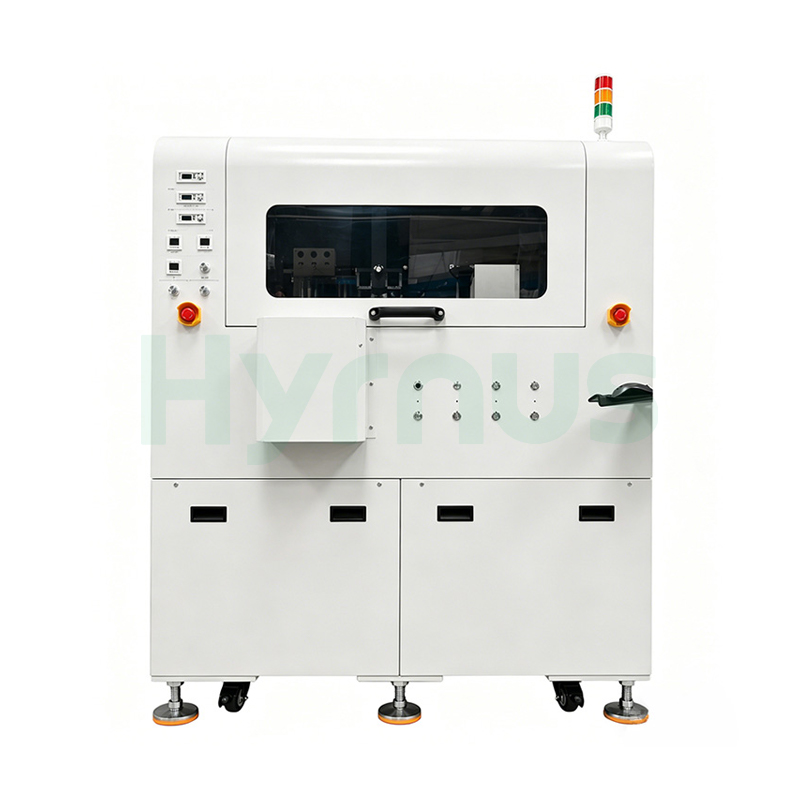
HY-ED010 Die Bonding Machine is a Die bonding machine developed for Automotive LED and Optoelectronic Semiconductor Packaging applications.
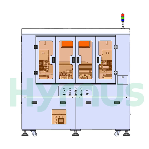
HY-ED007 Die Attach Machine is a High-Precision Die attach machine developed for Optical Communication, Optical Modules, Multi-Chip Modules (MCM), 3D Packaging, and Optoelectronic Device applications.
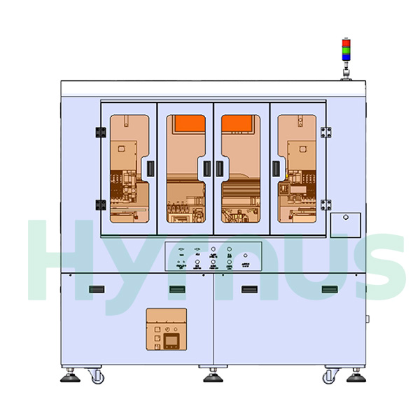
HY-ED003 Die Attach Equipment is a High-Precision Eutectic Bonder developed for Optical Communication, Optical Modules, Multi-Chip Modules (MCM), 3D Packaging, and Optoelectronic Device applications.
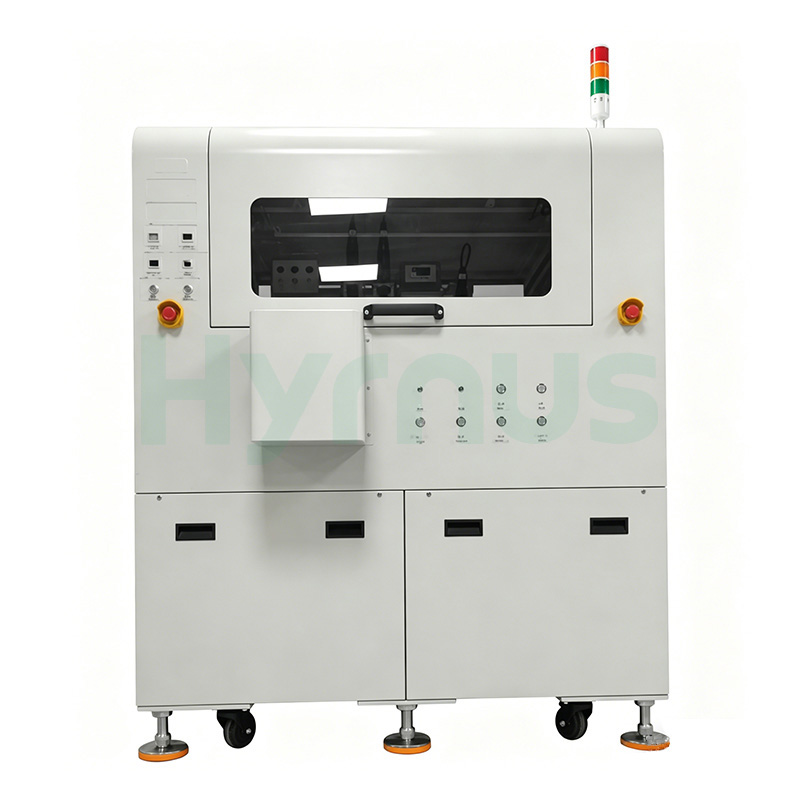
HY-DB504 Die Bonder is a Fully Automatic Die Bonder developed for Ultra-High-Precision Optoelectronic and Semiconductor Packaging applications.
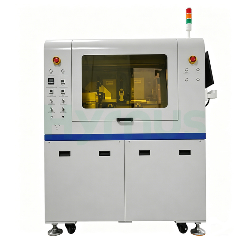
HY-DB503 Die Bonder is a High-Speed Fully Automatic Die Bonder developed for Optoelectronic and Semiconductor Packaging applications.
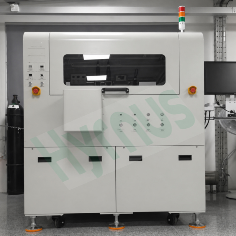
HY-DB501 Die Bonder is a fully automatic die bonder developed for ultra-high-precision optoelectronic and semiconductor packaging applications.It delivers precision-driven die attachment for optoelectronic packaging, targeting TO‑series devices, photodiodes, lasers, optocouplers, and miniLEDs with placement accuracy of ±5 μm and angular control within ±1°.
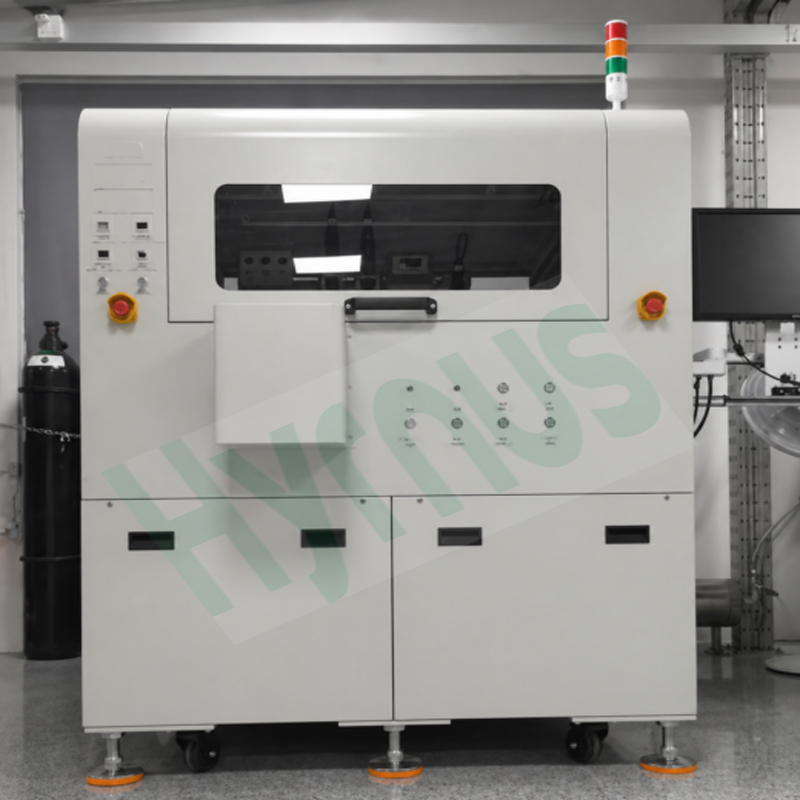
HY-DB500 Die Bonder is a high-end, fully automatic die bonder engineered for optoelectronic devices and high-precision semiconductor packaging. Built with exceptional stability, intelligent control, and a modular architecture, it is ideally suited for high-volume production of TO-series devices, photodiodes, lasers, optocouplers, miniLEDs, and consumer optoelectronic components.
leave a message
Scan To Wechat :

Scan To WhatsApp :