What Are You Looking For?


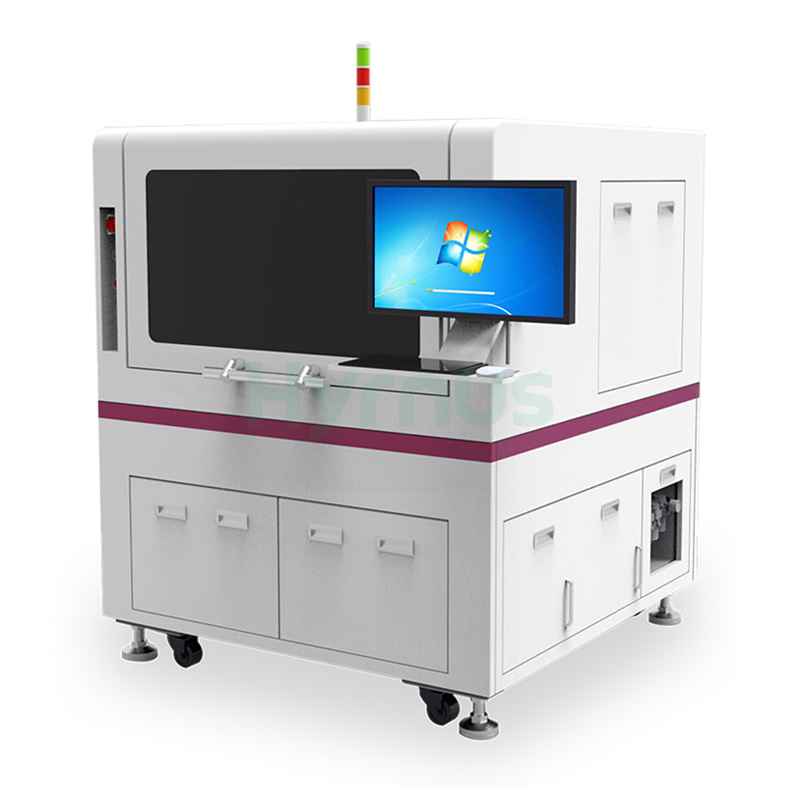
HY-PD12 Die Bonder is a high-precision panel-level die bonding system specifically designed for FOWLP/PLP advanced packaging processes, widely used in high-performance computing/AI chips, 5G/mmWave RF devices, SiP solutions, and Mini/Micro LED display panels.
Brand :
HYRNUSItem No. :
HY-PD12Order(MOQ) :
1 SetWarranty :
One-Year Warranty and Lifetime MaintenancePayment :
T/TLead Time :
7-35 DaysProduct Origin :
ChinaHigh Precision Panel-Level Packaging Die Bonder

Product Introduction
HY-PD12 Die Attach Machine achieves a bonding cycle of 250 ms with throughput of 14K UPH, delivering X/Y accuracy of ±25 μm and rotation accuracy of ≤ ±3°. The system handles 12" wafers with chip sizes from 0.2 × 0.2 mm to 3 × 3 mm and chip thickness ≥100 μm, supporting substrate sizes of 340 × 340 mm with thickness of 0.2–4 mm. Equipped with a 1280 × 1024 pixel camera offering recognition accuracy of 2.4 μm, the system features surface pick method with pick force of 30–250 g, bonding travel of 350 × 350 mm, and achieves position accuracy of ±2 μm and repeatability of ±1 μm. Operating on 220V / 50Hz with rated power of 1.0 kW and requiring compressed air of 0.6–1.0 MPa, the HY-PD12 delivers reliable, high-precision performance for heterogeneous integration and high-density interconnection in next-generation electronics manufacturing.
Technical Specifications
| Parameter | P8 | P12 | P8 Pro | P12 Pro | P12 Max |
| Operating System | Windows 7 | ||||
| Bonding Cycle (ms) | 200 | 250 | 500 | 1000 | |
| UPH | 18k | 14k | 6-8k | 3-5k | |
| X/Y Accuracy (μm) | ±25 | ±15 | |||
| Rotation Accuracy (°) | ≤±3 | ≤±0.5 | |||
| Wafer Size | 8" | 12" | 8" | 12" | 12" |
| Chip Size (mm) | 0.2x0.2~3x3 | 1x1~6x6 | |||
| Chip Thickness (μm) | ≥100 | ||||
| Substrate Size (mm) | 500x200 | 340x340 | 685x650 | ||
| Substrate Thickness (mm) | 0.2-4 | 0.2-2 | |||
| Image Resolution | 1280x1024 | 2592x1944 | |||
| Recognition Accuracy | 2.4μm | 1.2μm | |||
| Pick Method | Surface | Surface+Align | |||
| Pick Force (g) | 30-250 | 20-250 | |||
| Bonding Travel (mm) | 510x210 | 350x350 | 700x660 | ||
| Position Accuracy (μm) | ±2 | ±1 | |||
| Repeatability (μm) | ±1 | ||||
| Voltage | 220V/50Hz | ||||
| Compressed Air (MPa) | 0.6-1.0 | ||||
| Vacuum Input (KPa) | -0.6~-1.0 | ||||
| Power (kW) | 0.8 | 1 | 1.2 | 1.35 | 1.35 |
Application Scenarios
This panel-level package die bonder is specialized for FOWLP/PLP advanced packaging processes. It is widely used in the die attach of high-performance computing/AI chips, 5G/mm Wave RF devices, SiP/system-in-package solutions, and Mini/Micro LED display panels, enabling heterogeneous integration and high-density interconnection for next-generation electronics.
Product Details
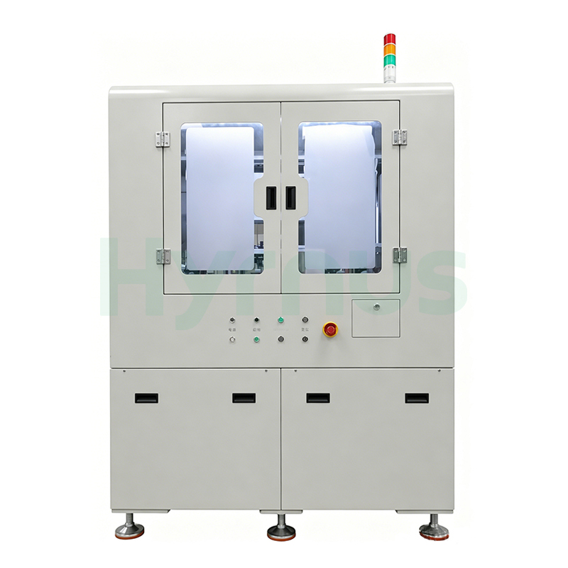
HY-ED022 Die Bonder is developed for Optical Communication and Optical Device Packaging applications.
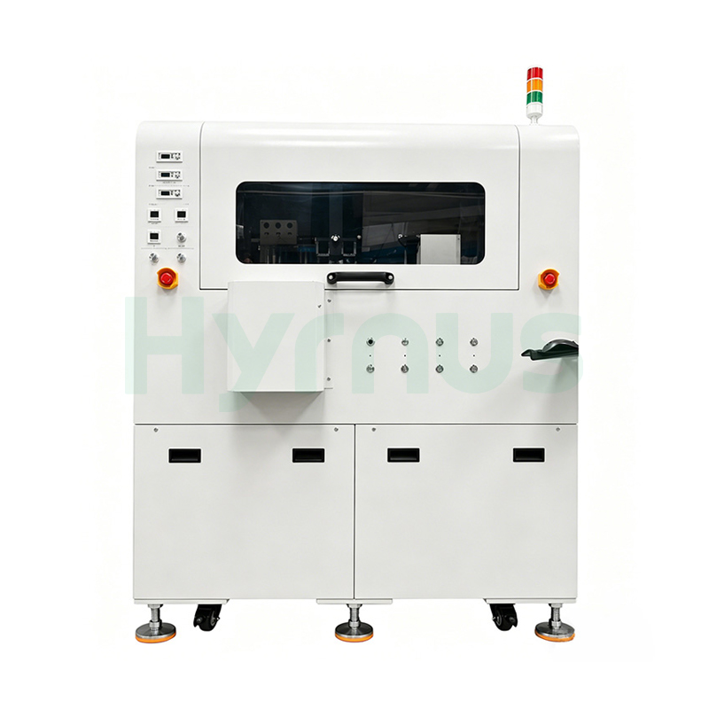
HY-ED010 Die Bonding Machine is a Die bonding machine developed for Automotive LED and Optoelectronic Semiconductor Packaging applications.
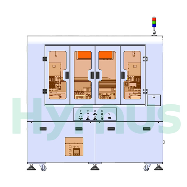
HY-ED007 Die Attach Machine is a High-Precision Die attach machine developed for Optical Communication, Optical Modules, Multi-Chip Modules (MCM), 3D Packaging, and Optoelectronic Device applications.
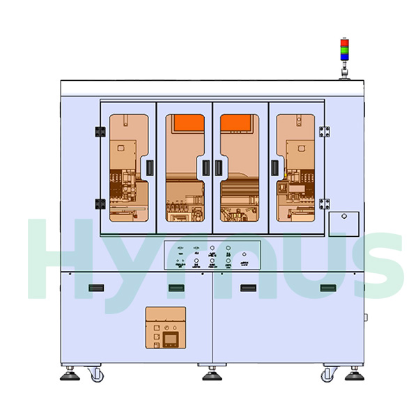
HY-ED003 Die Attach Equipment is a High-Precision Eutectic Bonder developed for Optical Communication, Optical Modules, Multi-Chip Modules (MCM), 3D Packaging, and Optoelectronic Device applications.
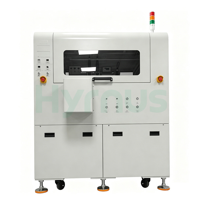
HY-DB504 Die Bonder is a Fully Automatic Die Bonder developed for Ultra-High-Precision Optoelectronic and Semiconductor Packaging applications.
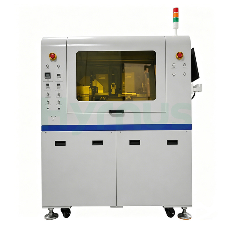
HY-DB503 Die Bonder is a High-Speed Fully Automatic Die Bonder developed for Optoelectronic and Semiconductor Packaging applications.
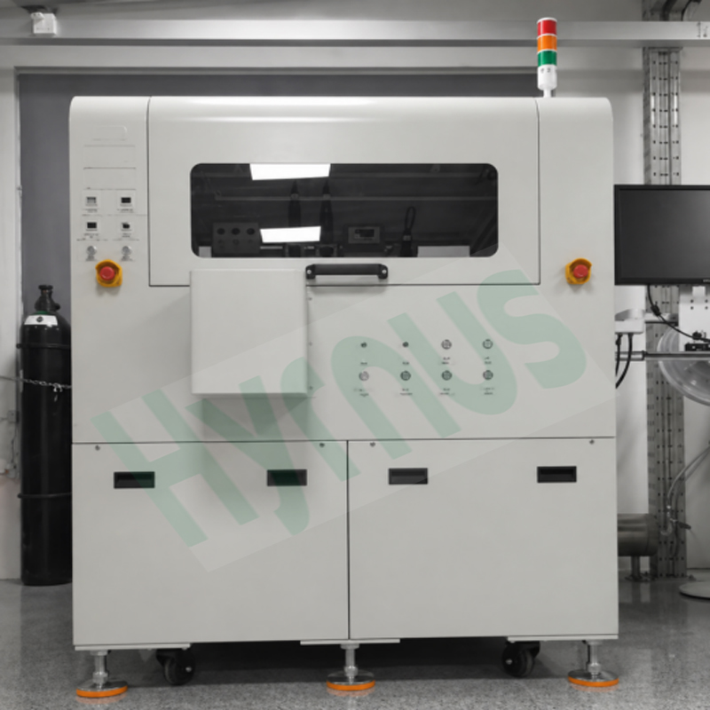
HY-DB501 Die Bonder is a fully automatic die bonder developed for ultra-high-precision optoelectronic and semiconductor packaging applications.It delivers precision-driven die attachment for optoelectronic packaging, targeting TO‑series devices, photodiodes, lasers, optocouplers, and miniLEDs with placement accuracy of ±5 μm and angular control within ±1°.
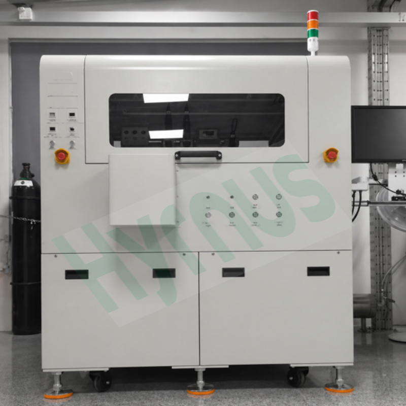
HY-DB500 Die Bonder is a high-end, fully automatic die bonder engineered for optoelectronic devices and high-precision semiconductor packaging. Built with exceptional stability, intelligent control, and a modular architecture, it is ideally suited for high-volume production of TO-series devices, photodiodes, lasers, optocouplers, miniLEDs, and consumer optoelectronic components.
leave a message
Scan To Wechat :

Scan To WhatsApp :