
Enter product details (such as color, size, materials etc.) and other specific requirements to receive an accurate quote.
leave a message
If you are interested in our products and want to know more details,please leave a message here,we will reply you as soon as we can.
other

Products


Semiconductor Manufacturing & Packaging Equipment

HYRNUS provides semiconductor manufacturing, packaging and testing equipment for research, pilot production and mass-production applications. Our equipment portfolio covers multiple processes from wafer preparation and die attachment to wire bonding, molding, inspection, testing and final sorting.

  • Oxygen Plasma Cleaner
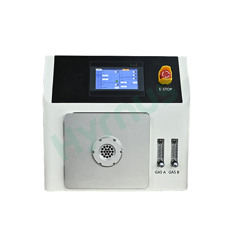
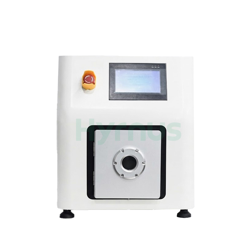
    2.5L Quartz Chamber Tabletop ICP Vacuum Plasma Cleaner for Laboratory Research
    HY-EB03H 2.5L tabletop ICP treatment unit is compact lab plasma surface treatment equipment with 13.56MHz RF power and dual gas channels. It generates high-density ICP plasma for cleaning, activating, etching and bonding materials, and is widely used for PDMS microfluidics, photoresist ashing and semiconductor lab research.  
    Read More

  • bbos wire bonding equipment
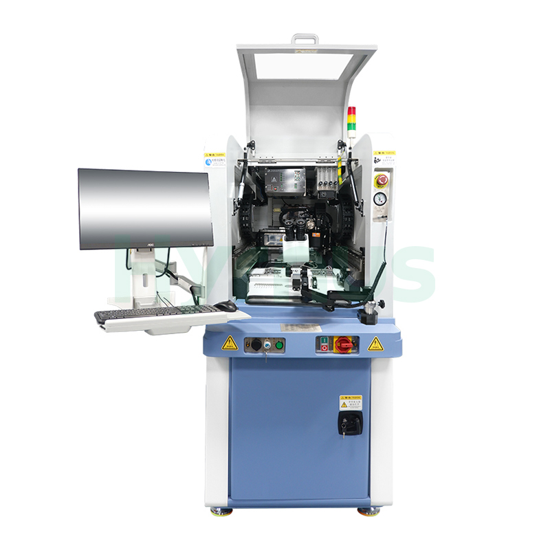
    MEMS Deep Access Wire Bonder BBOS Wire Bonding Equipment
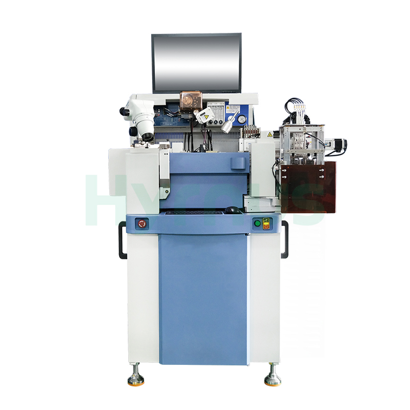
    The HY-WB800 Fully Automatic Deep Access Wire Bonder is designed for internal chip interconnection in advanced electronic packaging. It is widely used in hybrid circuits, MCM, MEMS, RF, microwave, optoelectronic, and automotive modules. It features real-time bonding and ultrasonic monitoring, precise loop control, EFO system, and high-stability wire feed for reliable high-end applications.
    Read More
  • ultrasonic wire bonding machine
    Semiconductor Ball Bonder Optical Communication Components Wire Bonding Machine
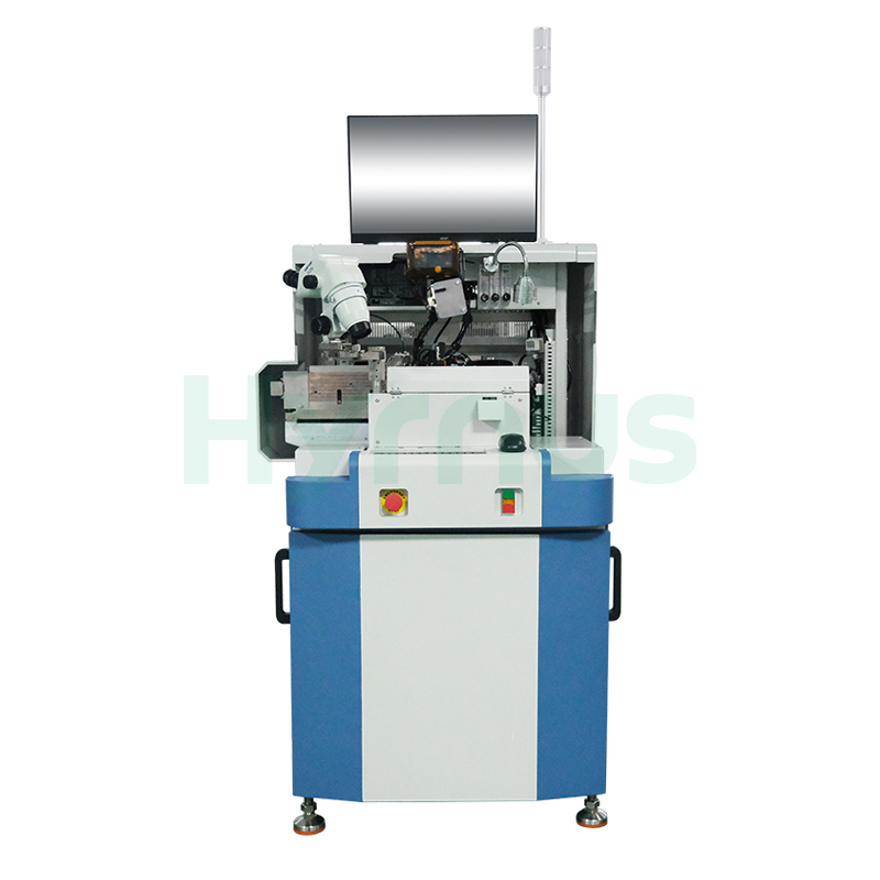
    The HY-WB400/HY-WB400P Wire Bonding Machine is a tilting and rotatable workholder wire bonding system designed for multi-planar interconnection in optical communication device packaging. It features automatic material handling, customizable fixtures, programmable optical path, and a high-precision XYZR direct drive system. With fast changeover and PR Look Ahead, it delivers high UPH and efficient production performance.
    Read More
  • 165L Chamber Vacuum Plasma Cleaner
    Industrial Production Vacuum Plasma Cleaner 165L Chamber for Semiconductor Packaging Mass Production
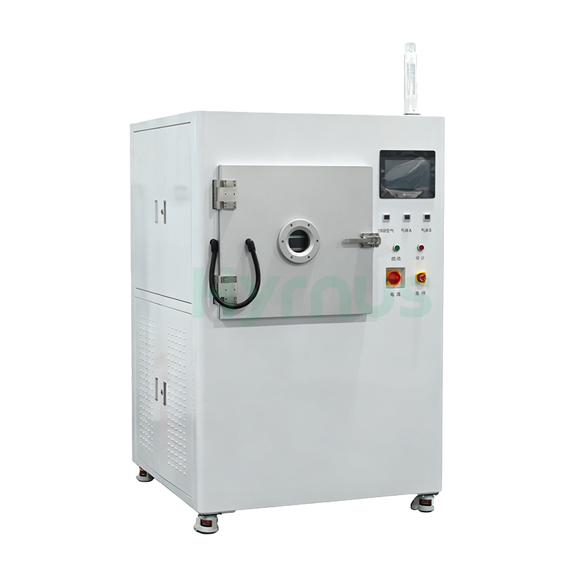
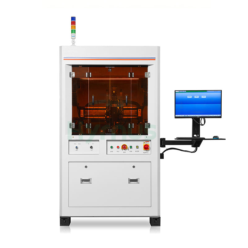
    This industrial vacuum plasma cleaner adopts 13.56MHz RF power and PLC touch control. Equipped with military-grade sealed chamber, dual plasma modes and dual adjustable gas channels, it stores up to 100 process recipes and delivers uniform plasma treatment.
    Read More
  • wire bonding equipment
    Fully Automatic Wire Bonder Ball Bonding Machine for Sensors, Lasers, Optical Devices
    The HY-WB700/HY-WB700P Fully Automatic Ball Wire Bonder is a standard planar wire bonding system designed for high-precision semiconductor packaging applications. It supports customizable rails, fixtures, and magazines. Equipped with dual-frequency transducer, auto-focus optical path, advanced motion control, and multi-stage EFO system, it ensures stable, efficient, and highly reliable bonding performance.
    Read More
  • aluminum wire bonding machine
    Full-Automatic Heavy Wire Bonder Power Module Wire Bonding Machine
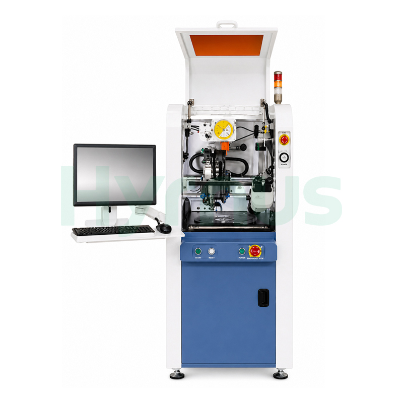
    HY-HW300 Full-Automatic Heavy Wire Bonder is designed for chip interconnection in advanced electronic components, widely used in power modules for EVs, renewable energy, rail transit, medical and aerospace systems. It features real-time bonding deformation and ultrasonic energy monitoring, closed-loop loop control, non-destructive testing, and high-precision automatic calibration for stable and reliable performance.
    Read More
  • Laboratory Plasma Surface Treatment Machine
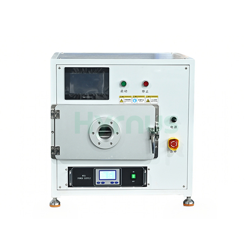
    Laboratory 25L Vacuum Plasma Cleaning Machine with 7-inch PLC Touch Screen
    HY-EL25H is a laboratory plasma treatment system widely adopted by research institutes, corporate R&D departments and small-batch pilot production lines. It adopts CCP (Capacitively Coupled Plasma) discharge technology. The complete system consists of a square stainless steel vacuum chamber, plasma generator, vacuum pump and gas inlet & exhaust ports. It effectively enhances substrate surface adhesion and improves surface hydrophilicity, with extensive applications in material bonding, coating, substrate film deposition and wafer bonding. This equipment delivers stable, repeatable plasma treatment for semiconductor, microfluidic and new material research projects.
    Read More
  • RF Vacuum Plasma Surface Treater
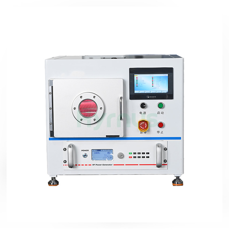
    13L CCP RF Vacuum Plasma Cleaner for Wafer Photoresist Stripping and Surface Activation
    HY-PS13 is a CCP vacuum plasma system dedicated to wafer photoresist stripping, cleaning and surface activation. Popular in research labs and small-batch semiconductor production, its stainless steel chamber full set with pump & gas modules improves material surface adhesion and hydrophilicity for bonding, coating and thin-film processes.
    Read More
  • Lab Plasma Cleaning Machine
    0–300W Continuously Adjustable Compact Vacuum Plasma Cleaning Machine for Laboratory R&D
    HY-ES10 is an experimental plasma treatment system, widely adopted by research institutes, universities, corporate R&D labs and low-volume production lines. It adopts CCP (Capacitively Coupled Plasma) discharge technology. The complete system consists of a vacuum chamber, plasma generator, vacuum pump, and gas inlet & exhaust ports. The treatment chamber is fabricated from square stainless steel.
    Read More
  • Atmospheric Pressure Plasma Cleaning Machine
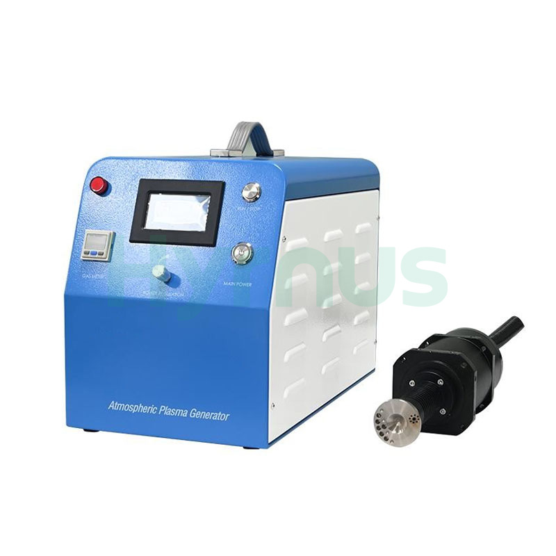
    High Efficiency Wide Temperature Atmospheric Pressure Direct Jet Plasma Cleaning Machine
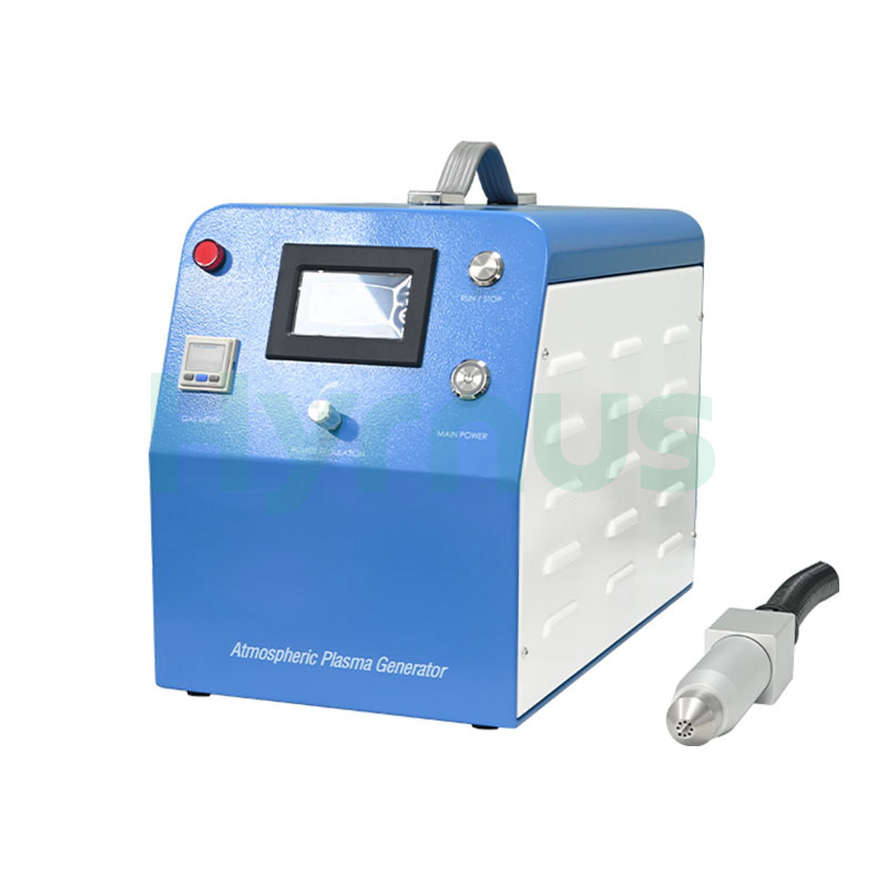
    HY-AR03 performs workpiece surface cleaning, activation and modification under ambient air. It optimizes substrate adhesion, hydrophilicity and printability, and removes organic residues, oil stains and oxide layers. Ideal as pre-treatment equipment for IC packaging, printing, bonding and coating processes, this compact unit supports inline automated production with low operating costs.
    Read More
  • Semiconductor Plasma Surface Treatment Machine
    Atmospheric Direct Jet Plasma Cleaner for IC Packaging Pre-treatment Surface Activation
    HY-AD03 is an atmospheric direct plasma cleaning device designed for surface cleaning, activation and modification under ambient air conditions. It features concentrated energy with a small treatment footprint, which effectively improves product adhesion, hydrophilicity and printability. It can also remove contaminants such as organic residues, oil stains and oxide layers from material surfaces.
    Read More
  • Automatic Terminal Ultrasonic Welding Machine
    Terminal Ultrasonic Welding Machine for Semiconductor Component Copper Lead Frame Production Line
    HY-UTB600 is a high-precision automatic ultrasonic welding equipment specially developed for power semiconductors, copper substrates, terminal wiring harnesses and busbars. It is widely applied in the welding process of metal terminals for power modules, copper lead frames and other electronic components. Featuring full automatic inline production capacity, it delivers outstanding performance in welding precision, production efficiency and low maintenance cost.
    Read More


One-Stop Semiconductor Equipment Solutions

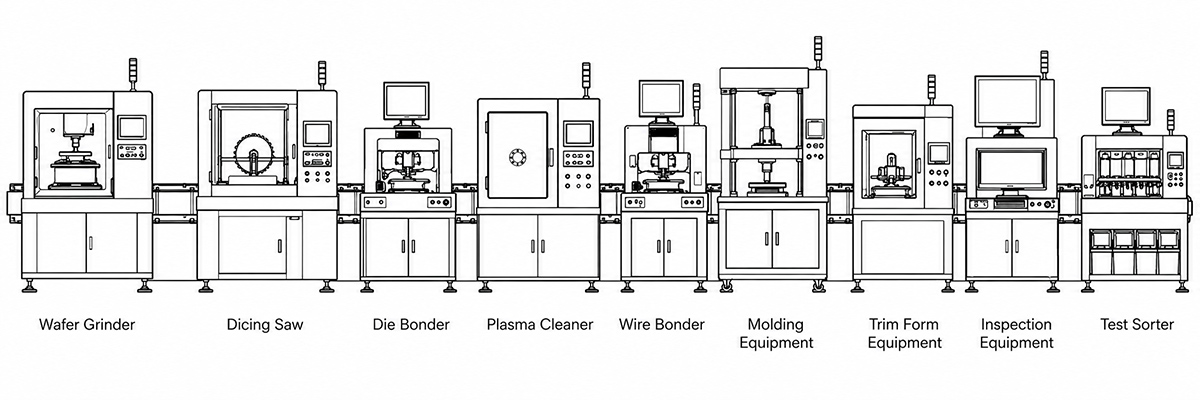
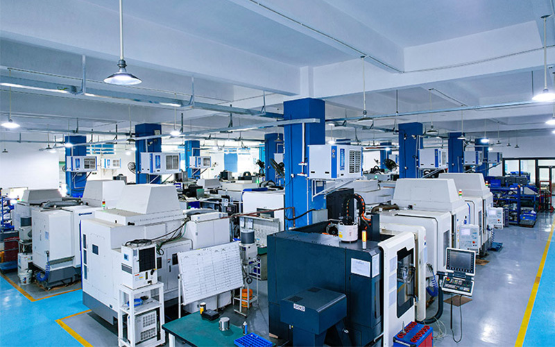
In addition to standalone semiconductor equipment, HYRNUS provides equipment configuration and integrated production line solutions for semiconductor manufacturing and electronic component packaging.


Get A custom solution
 

01

Production Line Planning

Plan the production process, equipment layout, material flow and workstation configuration based on the available factory space, target capacity and automation requirements.


02

Process Solution Development

Develop a suitable process flow according to the device type, package structure, materials and manufacturing requirements, covering key processes such as die attach, wire bonding, molding, inspection, testing and sorting.


03

Equipment Selection and Configuration

Select and configure suitable machines based on production capacity, material compatibility, positioning accuracy, process control, automation level and data traceability requirements.

Semiconductor packaging production line

leave a message

leave a message
If you are interested in our products and want to know more details,please leave a message here,we will reply you as soon as we can.
Contact us:allen@hyrnus.com