
Enter product details (such as color, size, materials etc.) and other specific requirements to receive an accurate quote.
leave a message
If you are interested in our products and want to know more details,please leave a message here,we will reply you as soon as we can.
other

Products


Semiconductor Manufacturing & Packaging Equipment

HYRNUS provides semiconductor manufacturing, packaging and testing equipment for research, pilot production and mass-production applications. Our equipment portfolio covers multiple processes from wafer preparation and die attachment to wire bonding, molding, inspection, testing and final sorting.

  • Integrated Ultrasonic Pin Torque Welding Machine
    Ultrasonic Pin Welder for Automatic Torque Welding Multi-Shape Terminals
    HY-UPB600 features full-process real-time monitoring of pressure, energy and welding time to guarantee stable welding quality, with fully automatic operation covering auto loading & unloading, automatic positioning and automated welding. It integrates a built-in product cleaning function, supports multi-angle welding ranging from 0° to 360°, and adopts a master-slave welding tip design that allows for fast replacement and reduces long-term consumable costs.
    Read More

  • Multi-functional Die Attach Equipment
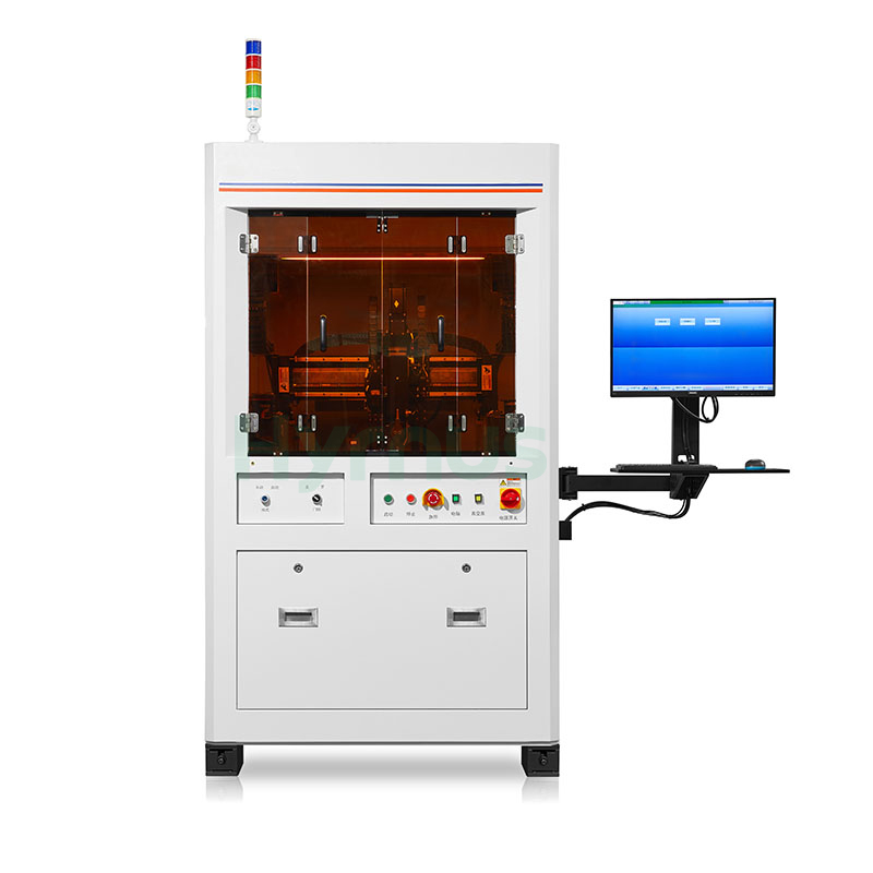
    High Precision Dual Worktables Eutectic Die Bonder Suitable for 6-inch Wafer Semiconductor Packaging
    HY-GD4000 handles both eutectic bonding and adhesive die attach for chip packaging. Equipped with dual bond heads and dual eutectic stages, it delivers high productivity with a 12-station automatic nozzle library. The independent ZR axis ensures precise component placement and consistent bonding pressure, while programmable multi-stage heating adapts to various eutectic alloys for multi-chip and flip-chip assembly. Its integrated vision system realizes automatic high-precision positioning and post-bond quality inspection.
    Read More
  • X Ray Inspection Machine
    Fast 3D CT X-Ray Inspection Equipment for Laminated Power Cell OH Detection
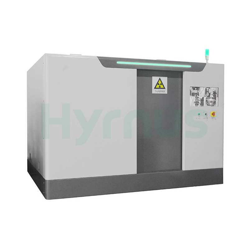
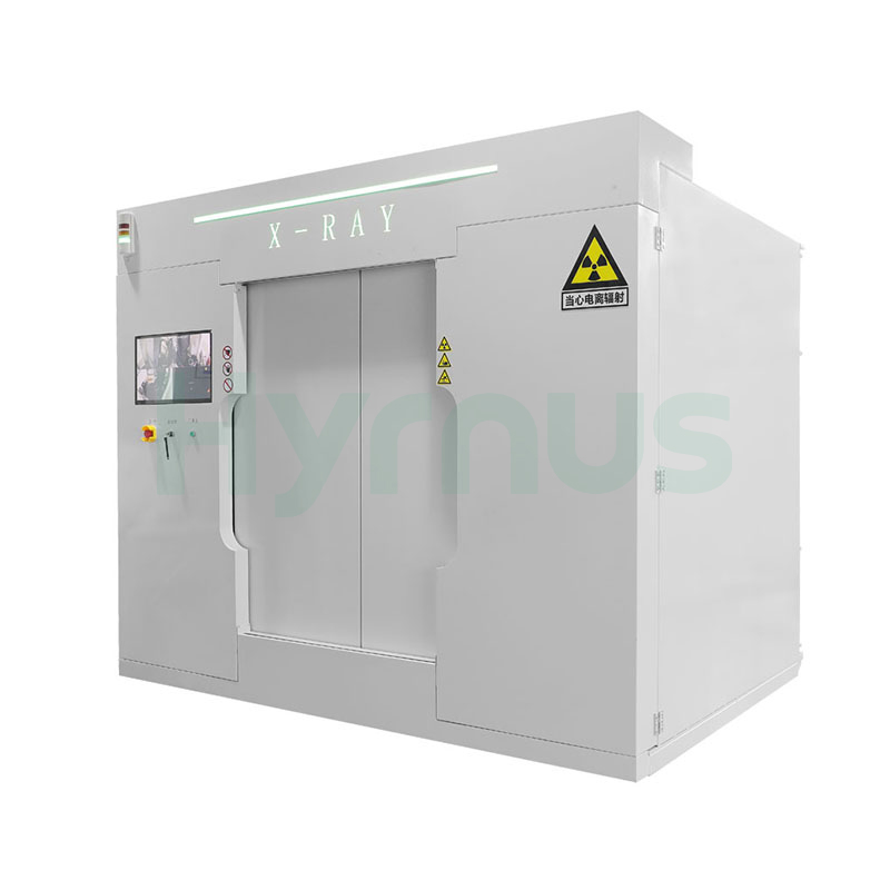
    HY-XRB8101 fast 3D CT X-Ray system adopts X-ray penetration to complete non-destructive Open Hole (OH) flaw inspection for laminated power cell corners. Multi-angle scanning generates complete 3D volumetric data, and built-in AI algorithms realize automatic defect judgment to stabilize quality control during mass new energy cell manufacturing.
    Read More
  • X Ray Inspection System
    Ultra High-Precision 3D Industrial CT for Multi-Industry Non-Destructive X-Ray Inspection
    HY-XR8001 supports offline scanning and imaging for product Regions of Interest (ROI). Following 3D reconstruction, our dedicated visualization analysis software delivers accurate analytical measurement. Ideal for in-process quality control, failure analysis and laboratory research, the system performs fully non-destructive testing to visualize internal product structures and hidden defects, with complete measurement and analytical capabilities.
    Read More
  • X Ray Inspection System
    Semi-Automatic X-RAY Inspection Equipment for Semiconductor IC Packaging and Electronic Capacitors
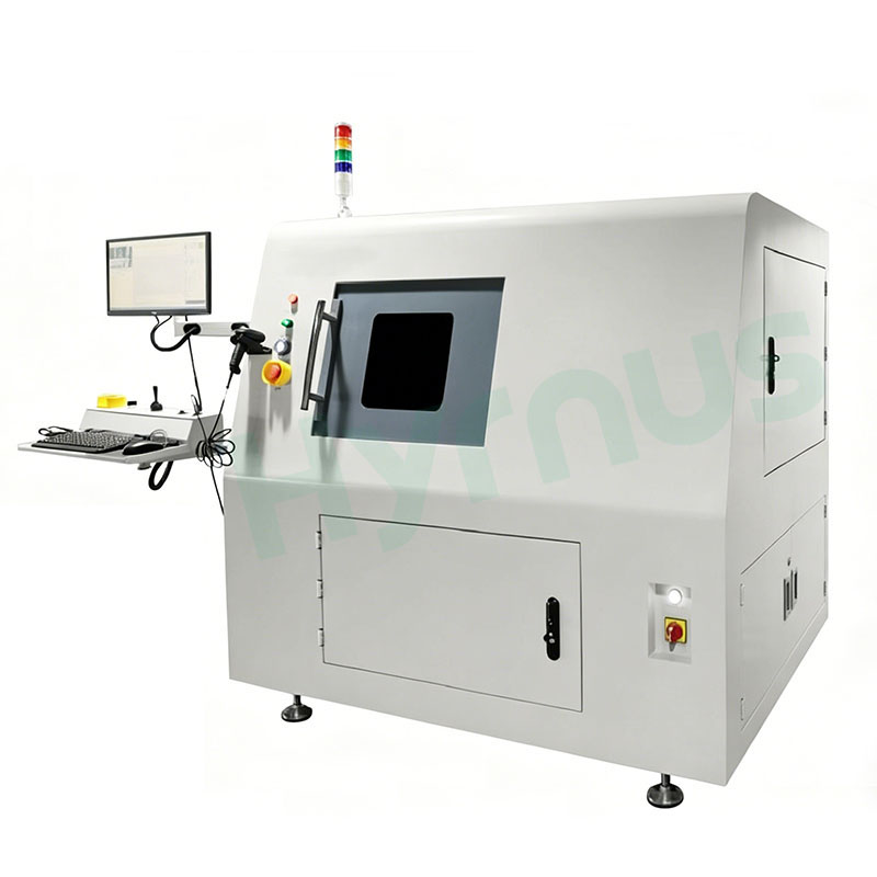
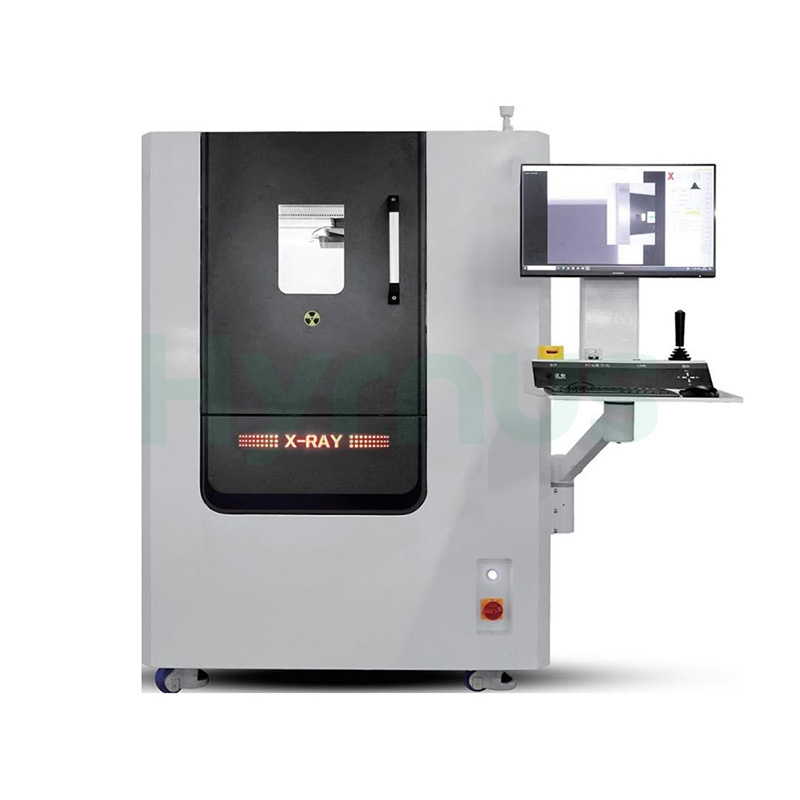
    HY-XR5010(2.5D) Series performs non-destructive testing for IC packaging, BGA/QFN chips, PCBA and capacitors. Equipped with CNC motion, multi-angle imaging and one-click void analysis, it detects voids, solder faults and dimensional errors. Three models fit small-batch checks, production sampling and lab R&D; optional barcode tracking and a high-res detector spot defects as tiny as 4μm. Full enclosed lead shielding limits radiation below 1μSv/h, with complete official radiation safety certifications.
    Read More
  • X Ray Inspection for Electronic Components
    Semi-Automatic X-Ray Inspection System for New Energy Batteries and Semiconductors
    HY-XR5010A  (2D) Series detects invisible internal flaws of industrial workpieces. It integrates micro-focus ray source, high-definition flat-panel imaging and CNC automatic inspection functions, equipped with reliable radiation protection design, suitable for offline quality control of medium-volume production lines across multiple manufacturing sectors.
    Read More
  • Automatic Plasma Surface Treatment Equipment
    Automatic 3-Axis Motion Platform Analog Low-Temperature Direct Injection Plasma Cleaner
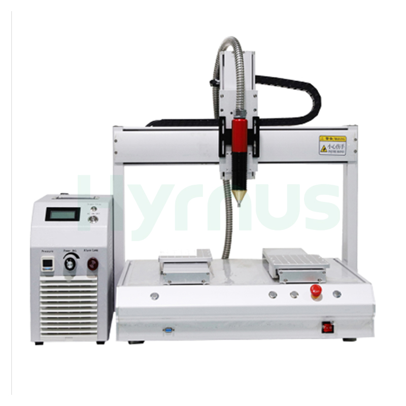
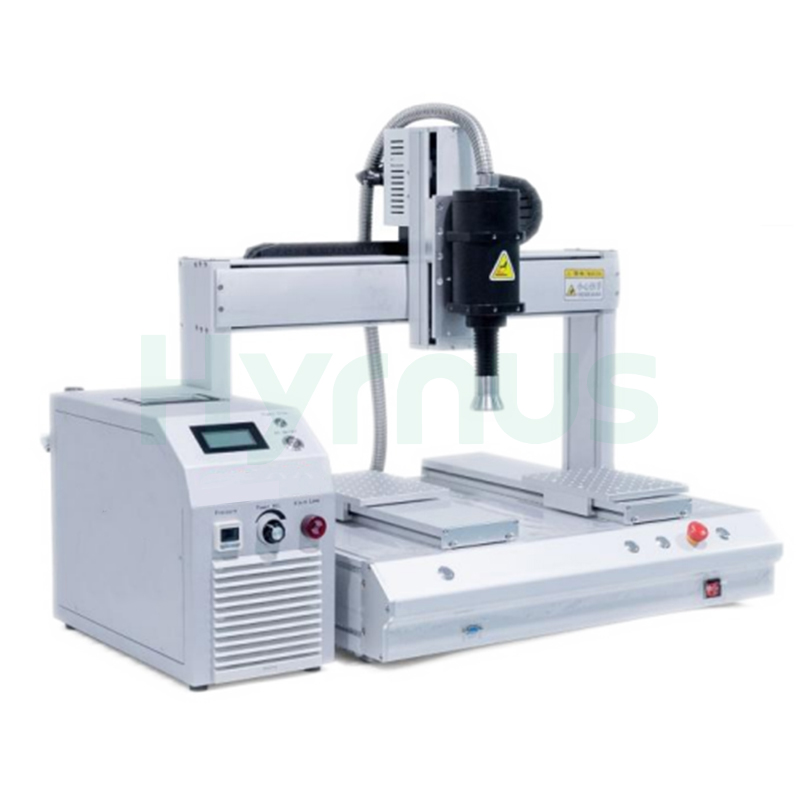
    HY-TM500 works under atmospheric pressure without vacuum chambers. Custom 3-axis rails deliver full-coverage precise treatment. Built with military-grade hardware and digital control, it supports 0–800W adjustable power. Zero-potential low-temperature plasma protects PCB, FPC and semiconductor components, completing surface cleaning, activation and modification to boost adhesion for bonding, printing and coating. It is ready for inline automation in 3C, display, semiconductor, automotive and new energy industries.
    Read More
  • Plasma Surface Treatment Machine
    1000W Adjustable Digital Rotary Circular Plasma Cleaning Machine for PCB Mass Line
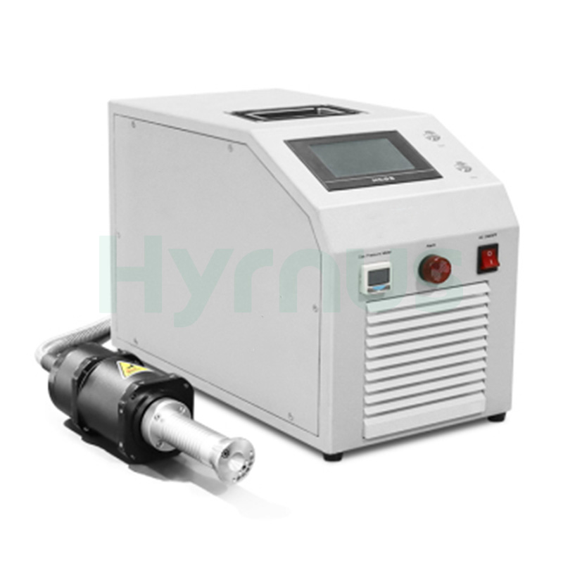
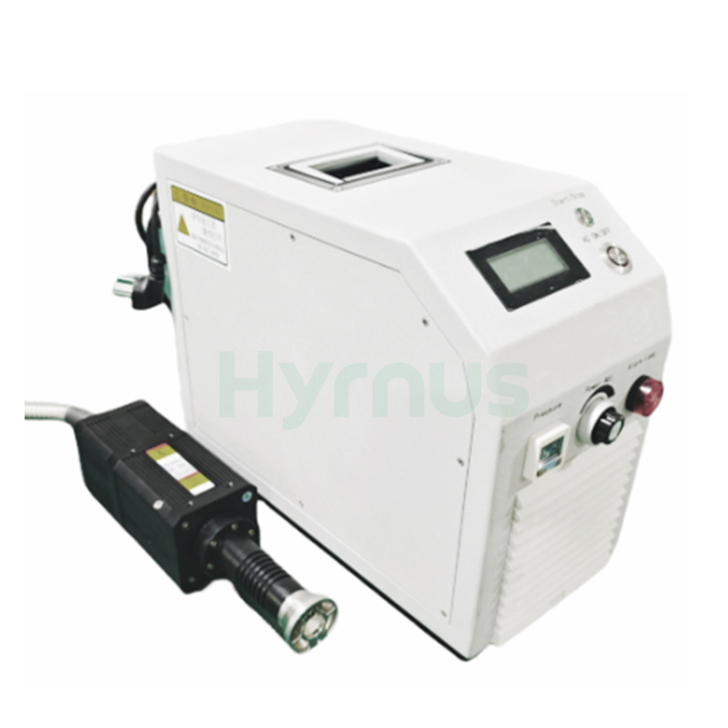
    HY-DC1000 is equipped with a wide coverage rotary gun and interchangeable nozzles ranging from 20 to 80mm, customized for large flat workpieces including full-size PCBs, new energy battery electrodes, automotive plastic components and display glass panels. It supports 0–1000W wide-range adjustable power to form uniform plasma coverage over large surfaces, efficiently stripping organic contaminants and eliminating printing voids & coating delamination issues for mass-production inline assembly lines.
    Read More
  • Plasma Surface Treatment
    600W Adjustable Digital Low-Temperature Direct Spray Plasma Cleaning Machine for Semiconductor Chips
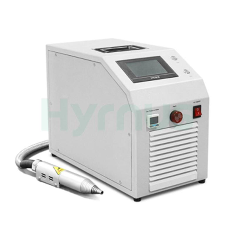
    HY-DD600 adopts narrow small nozzle design (2–6mm effective width), dedicated for tiny precision sensitive parts including chips, FPC flexible circuits, miniature BGA substrates. Zero-potential low-temperature plasma jet eliminates thermal burn risk for ultra-thin PI/ITO materials. Its compact gun fits narrow gaps and complex micro-structures, perfectly matching small automatic bonding & dispensing lines for semiconductor packaging and camera module pretreatment.
    Read More
  • Plasma Cleaning System
    1000W Adjustable Analog Rotary Platform Atmospheric Plasma Cleaner for Electronic Components
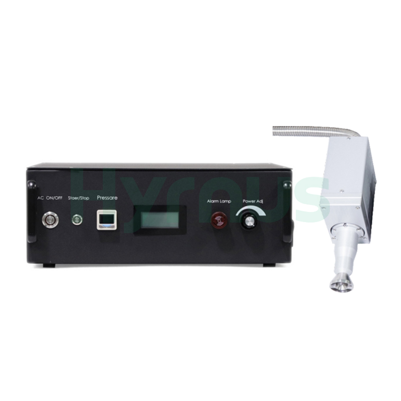
    HY-AC500 adopts rotary plasma spray gun and dual manual & I/O control modes, realizing uniform cleaning, activation and micro-etching for PCB, FPC, BGA and semiconductor chips. It features military-grade hardware, digital real-time monitoring and multi-layer safety protection. This desktop 1000W analog plasma machine is widely used for pre-treatment in semiconductor packaging, 3C electronics, display, automotive electronics and new energy industries.
    Read More
  • Plasma Surface Treatment Equipment
    Horizontal Inline Rotary Atmospheric Plasma Cleaner for Continuous Production of Substrates and Lead Frames
    HY-AC1000H uses vacuum-free low-temperature neutral plasma, fitted with customizable rails and dual rotary guns. With 0–1000W adjustable power and 20–80mm treatment width, it safely cleans chips without thermal damage. Combined physical & chemical dry cleaning enhances bonding for die attach, wire bonding and molding to reduce delamination and voids. Supporting manual & IO control with full safety monitoring, it connects to auto lines for continuous processing of substrates, lead frames and large FPC panels, delivering stable long-hour full-load production with response time below 0.1s.
    Read More
  • Atmospheric Low-Temperature Rotary Square Plasma Cleaner
    Atmospheric Low-Temperature Rotary Square Plasma Cleaner for IC Packaging and Semiconductor Testing
     HY-AS1200 is fitted with a motor-driven rotating nozzle to create an even plasma surface. With a treatment width of 20–80 mm and adjustable power ranging from 0 to 1200 W, it perfectly matches batch pre-treatment of large-area lead frames and substrates. The room-temperature neutral plasma will not damage chips, dry removing organic residues and surface oxides under atmospheric pressure to strengthen adhesion for die attach, wire bonding and molding while cutting delamination and void defects. Equipped with multi-layer safety protection and fully compatible with automated production lines, this equipment is widely used in packaging and testing procedures for ICs, FPCs and automotive chips.
    Read More


One-Stop Semiconductor Equipment Solutions

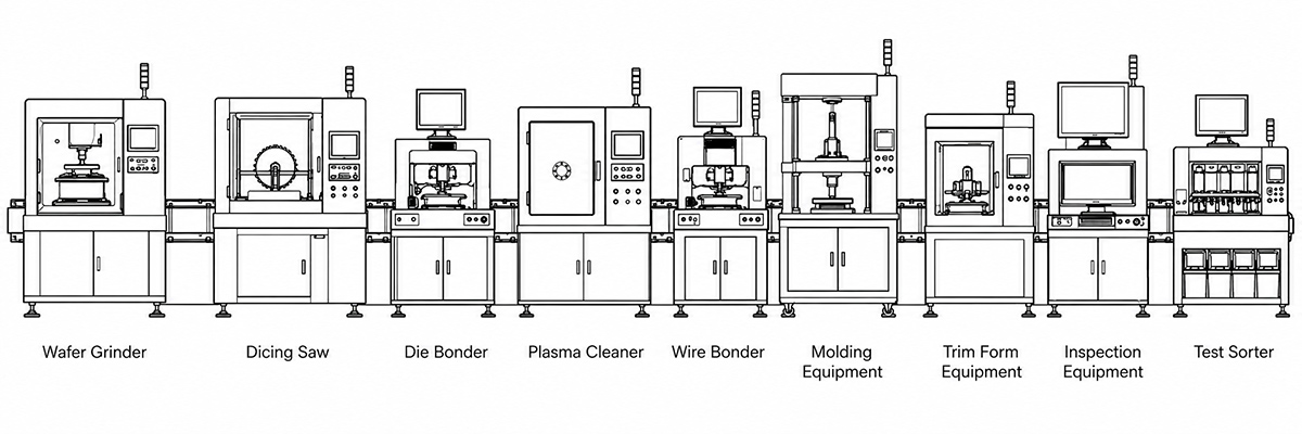
In addition to standalone semiconductor equipment, HYRNUS provides equipment configuration and integrated production line solutions for semiconductor manufacturing and electronic component packaging.


Get A custom solution
 

01

Production Line Planning

Plan the production process, equipment layout, material flow and workstation configuration based on the available factory space, target capacity and automation requirements.


02

Process Solution Development

Develop a suitable process flow according to the device type, package structure, materials and manufacturing requirements, covering key processes such as die attach, wire bonding, molding, inspection, testing and sorting.


03

Equipment Selection and Configuration

Select and configure suitable machines based on production capacity, material compatibility, positioning accuracy, process control, automation level and data traceability requirements.

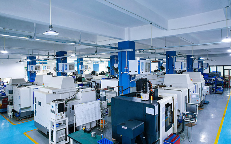
Semiconductor packaging production line

leave a message

leave a message
If you are interested in our products and want to know more details,please leave a message here,we will reply you as soon as we can.
Contact us:allen@hyrnus.com